

The Defect Explosion: Why Classification Is Moving to the Edge
As semiconductor processes move below 2nm and device architectures become more complex, manufacturers need greater inspection sensitivity to identify smaller and more subtle defect signals. That sensitivity also captures normal process variation and nuisance signals that may resemble defects, increasing the number of events requiring classification. Millions of events may therefore be detected on a single wafer, even as overall yield improves.
Today’s challenge goes well beyond finding anomalies alone. Fabs must determine which events are most likely to impact yield and respond quickly. When inspection data outpaces the systems used to transfer and classify it, engineers face delayed results, heavier review workloads and less time to act on the defects that matter most.
To manage growing defect volumes, manufacturers are increasingly moving automatic defect classification closer to where inspection data is generated. Often referred to as edge AI, this approach performs classification on or near the inspection tool rather than relying exclusively on centralized processing.
More Data, Less Time to Decide
Inspection systems generate on-the-fly, review and whole-wafer images for different applications. As sensitivity improves, the resulting data stream includes not only defects of interest but normal process variation and nuisance detections that require classification (Figure 1).
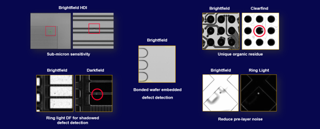
Figure 1: Brightfield, darkfield, high-speed infrared, Clearfind® and ring light imaging provide manufacturers with complementary views for detecting defects across diverse materials, structures and process conditions.
At advanced nodes, nuisance or low-value signals may represent 70% to 90% of detected events. Traditional die-to-die and reference-image approaches can struggle when normal process variation begins to resemble a defect. This creates a difficult tradeoff: manufacturers can reduce sensitivity and risk missing a critical defect or preserve sensitivity and send an overwhelming number of nuisance events into classification and review.
Left unresolved, overkill can consume review capacity and drive unnecessary disposition decisions, while underkill can allow defects to escape. Both outcomes slow learning and make it harder to focus engineering resources on process excursions requiring action.
When Classification Becomes a Bottleneck
The volume of image data moving through the fab compounds the problem. In a conventional workflow, inspection images are transferred for classification, classification results are returned to the inspection process and the final defect information is exported to the fab’s defect management environment.
As inspection throughput and defect counts rise, network transfer and centralized processing may not keep pace. Even when server performance improves, transferring large volumes of inspection images for centralized classification can create delays that slow decision making and yield learning. As process complexity increases, it becomes more difficult to distinguish critical defects from normal process variation and nuisance signals.
Bringing Automatic Defect Classification On Tool
With edge AI, manufacturers can change the workflow by bringing AI-based automatic defect classification (ADC) closer to the inspection process or directly onto the tool. Classifying images where the data is generated can reduce nuisance events before they move downstream and help results keep pace with production.
Onto Innovation’s TrueADC® software combines deep learning, real-world defect modeling and a proprietary hybrid decision-making process. Its multi-engine approach combines traditional and deep-learning classification methods to reduce overkill and underkill, while results that cannot be confidently classified are flagged as unknown for engineer review rather than forced into a potentially incorrect class.
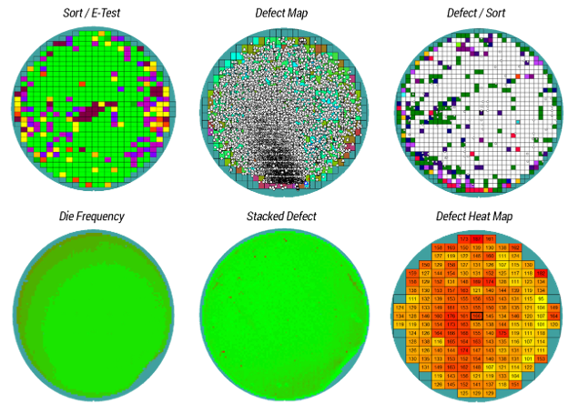
TrueADC software integrates with Onto Innovation automated optical inspection systems as well as Discover® Defect and Discover Review software (Figure 2). In an on-tool workflow, AI-based classification helps preserve sensitivity to defects of interest while reducing unnecessary image transfer and manual review.
Figure 2: Discover® Defect software offers a comprehensive mapping suite that covers all aspects of semiconductor processes, enabling manufacturers to transform classification results into actionable process insights.
Connecting Classification, Review and Analysis
Classification creates greater value when it is connected to review and defect analysis. Discover Defect software provides centralized defect data management and analysis, while Discover Review software enables offline review and classification of results from connected inspection tools.
Together, these capabilities create a feedback loop in which engineers can review unknown or misclassified defects, update model libraries, monitor key performance indicators and identify changes in defect behavior. The goal is to turn a large population of detected events into a more useful set of yield-relevant information for process control.
Building Models Around the Fab’s Process
Effective classification depends on representative training data. Engineers build and validate models using labeled libraries of known defects, nuisance conditions and relevant process variation. Customer images and process data must remain within the fab’s intellectual property and data-governance requirements.
Onto Innovation can supplement application- and fab-relevant training with semiconductor-domain model knowledge, including established defect characteristics and simulated examples. This foundation can reduce the number of image samples required during model development, while process context helps determine which events are meaningful.
Human Oversight Remains Essential
On-tool classification does not remove engineers from the process. During model development, teams collect, label and validate representative images. After deployment, operators review unknown or previously unseen defects, correct misclassifications and use those results to guide model updates.
Because processes and defect populations change, fabs also need key performance indicator (KPI) monitoring, anomaly alerts and clear retraining criteria. Edge AI is not a set-it-and-forget-it system. Continuous oversight keeps classification aligned with changing process conditions and production priorities.
Better Decisions
The explosion in detected events and nuisance signals is ultimately a decision-making challenge. Manufacturers need to maintain inspection sensitivity without allowing nuisance signals and data-transfer delays to overwhelm review and process control workflows.
By bringing automatic defect classification closer to inspection and connecting TrueADC software with Discover Defect and Discover Review software, Onto Innovation helps manufacturers reduce nuisance workload, prioritize yield-relevant defects and act on inspection results sooner, giving engineers clearer, more consistent information so they can accelerate yield learning and keep production moving.
Prasad Bachiraju is a Sales Account Senior Director at Onto Innovation.
You Have a Challenge? Let’s talk.
We’d love to connect with you.
Looking to learn more about our innovative solutions and capabilities? Our team of experts is ready to assist you. Reach out today and let’s starts a conversation about how we can help you achieve your goals.
Let’s Talk
"*" indicates required fields