CnCV® System

The CnCV system enables wafer-level characterization of WBG materials without test device fabrication, reducing time and cost. As a mercury-free alternative to MCV, it eliminates contamination concerns. The enhanced Kinetic CV mode with UV-assisted corona charge neutralization achieves high throughput and precision for fast, reliable process control.

CnCV-230-NEW

Product Overview

The CnCV system utilizes a novel constant surface potential corona charging, which enables the precision required over a large voltage range. The patented technology includes charge- and photo-assisted modes, especially suited for speed and precision on WBG materials and structures, including SiC, Ga2O3, GaN, and AlGaN/GaN HEMT. Additionally, Corona-Kelvin characterization includes electrical properties of dielectrics and interfaces of films on SiC and GaN epi layers. An automated top-side edge contact (TSEC) is also available enabling characterization of WBG on insulating/semi-insulating substrates. Automated bias-temperature stress (BTS) measurements are also available with the CnCV system, providing a fast, noncontact way to quantify the reliability of passivated SiC and GaN. 

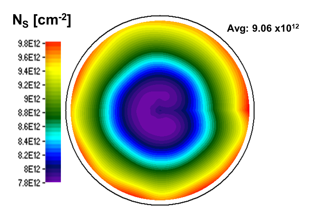
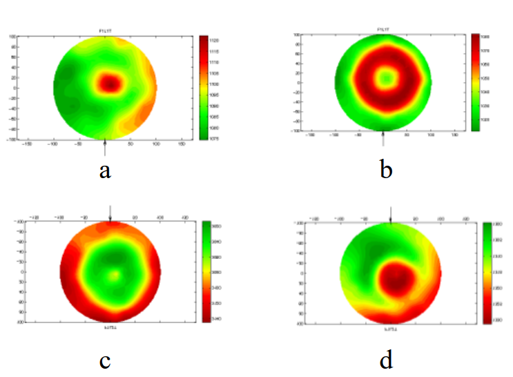
Beyond typical CV type parameters, the full wafer corona approach allows for QUAD (quality, uniformity, and defect) mapping. The electrical defect imaging, QUAD-EDI, mode is especially designed for SiC. It provides a unique means for quick screening of epi electrical defectivity enabling improvement in device yield prediction. 

Figure 1. QUAD-EDI Map on final metallized device wafer after Merged Schottky PiN diode fabrication identifying failed dies.

Applications

  • Non-contact epi dopant depth profiling in WBG materials
  • AlGaN\GaN HEMT measurements (pinch off voltage & 2DEG sheet charge)
  • Dielectric and interface characterization electrical defect imaging in SiC for yield prediction
  • Bias-temperature stress (BTS) instability measurements on passivated WBG materials
Related Products
View all
FAaST® Digital SPV _feat

FAaST® Digital SPV System 

The FAaST Digital Surface PhotoVoltage (SPV) system delivers leading sensitivity for silicon wafer contamination control, rapidly mapping minority carrier diffusion length and detecting economically impactful iron (Fe) in minutes.
View Product
FAaST® CV_IV System _feat

FAaST® CV/IV System 

The FAaST systems deliver versatile, non-contact electrical metrology for process control and development of semiconductor materials and devices.  They provide a broad range of parameters characterizing wafers, dielectrics and interfaces.
View Product
Related Insights & Resources
View all
cmcv 0404826

A Review of Recent Technological Advancements in Corona Noncontact Metrology Tools, CnCV, for Industrial WBG Wafer Testing and Electrical Defect Related Yield Prediction 

Learn more

Do you have a CnCV system question? Let’s talk!

As your partner for innovative solutions, we’re always here for you.

Discover how our cutting-edge semiconductor solutions are engineered to meet your most complex challenges: delivering performance, reliability and innovation where it matters most.

Let’s Talk

"*" indicates required fields

This field is for validation purposes and should be left unchanged.

Atlas® G6 System

The Atlas G6 system is an OCD and thin film metrology tool engineered for the most advanced logic and memory devices. Designed to meet the demands of next-generation AI applications and beyond, it delivers enhanced optics, AI-driven recipe development, and tighter tool matching for superior process control.

Atlas-G6-NEWBRAND

Product Overview

As semiconductor manufacturers push into next-generation GAA nodes and next-gen HBM and vertical DRAM architectures, process control requirements are tightening. Smaller nanosheet structures and denser DRAM cells demand higher measurement precision, faster recipe development, and tighter tool-to-tool matching.

The Atlas® G6 system is engineered to meet these challenges with a new optics design that improves signal-to-noise ratio, spectral stability, and measurement precision. Enhanced software algorithms and data management tools deliver better fleet-wide spectra matching, while a new data channel and next-generation model-guided machine learning in Ai Diffract™ software enable faster, more robust recipe development. A smaller optical spot size ensures accurate measurements on today’s most compact DRAM structures.

Fully integrated with Onto Innovation’s Discover® ecosystem, the Atlas G6 system empowers fabs with predictive process control and smart manufacturing capabilities—accelerating yield and time to market for the industry’s most advanced devices.

Applications

  • OCD for litho, etch, CVD & CMP process in all device segments
  • Local variation
  • Asymmetry and tilt
  • Common and critical films
  • Stress & wafer warpage
Related Products
View all
impulse v_feat

IMPULSE® V System

Advanced high throughput integrated metrology system with AI-driven machine learning option. The system offers maximum sensitivity and accuracy to CMP process excursions and enables process engineers to establish APC control with high-accuracy feedback.
View Product
impulse+_feat

IMPULSE®+ System

Integrated metrology system offering maximum sensitivity and accuracy to CMP process excursions and enabling process engineers to establish APC control with high-accuracy feedback.
View Product
aspect_feat

Aspect® System

Advanced infrared optical critical dimension (IRCD) metrology system for high aspect ratio structures in 3D NAND, 2D & 3D DRAM, CIS and power devices.
View Product
ocdsolutions_aidiffract_feat

OCD Solutions

A suite of OCD modeling software and computing hardware offering comprehensive capabilities for inline metrology, offline recipe creation and fleet management.
View Product
Related Insights & Resources
View all
dec 2025 blog

Smaller Geometries, Bigger Demands: The Role of OCD in GAA Logic and Vertical Gate DRAM Process Control 

Learn more

Do you have an Atlas G6 system question? Let’s talk!

As your partner for innovative solutions, we’re always here for you.

Discover how our cutting-edge semiconductor solutions are engineered to meet your most complex challenges: delivering performance, reliability and innovation where it matters most.

Let’s Talk

"*" indicates required fields

This field is for validation purposes and should be left unchanged.

Inspection Tool Productivity Software

The native integration of the Discover software platform boosts tool throughput and enhances inspection quality by capturing more defects of interest. It provides a complete reduced review solution utilizing advanced machine learning (ML) and artificial intelligence (AI) technologies, customized to meet unique customer needs.

Enhance Your Inspection & Metrology Experience with Onto Software

Optimized Image Capture for Inspection Tools
Discover software enhances inspection quality and tool throughput by optimizing the image capture sample plan.

AI-Powered Automatic Defect Classification (TrueADC Software)
Integrated AI-based classification improves device quality and yield, driving fab efficiency and productivity.

Streamlined Review Software
Reduced review best practices improve operator productivity, enhance engineering review quality, and shorten review time.

Advanced Defect Analytics
Comprehensive inline wafer/panel monitoring enables automatic alarm notifications, detailed reports and Out-of-Control Action Plans (OCAPs).

Defect Source Analysis
Enables actionable process feedback to improve manufacturing outcomes.

Automated Business Analysis with Report Server
Boosts engineering productivity by up to 25% and supports multiple production report formats.

Machine Learning-Based Pattern Detection
The Discover Patterns software module proactively identifies wafer-level systematic yield-limiting issues and classifies them for analytics, enabling both process feedback and feedforward.

Centralized Defect & Metrology Management
Built on a scalable Big Data and high-availability architecture, this solution supports advanced applications such as high volume manufacturing (HVM) bump metrology, capable of handling wafers with over 100 million bumps.

Related Products
View all
dragonflyg5_feat

Dragonfly® G5 System

The latest generation inline pattern inspection system in the Dragonfly series, delivering sub-micron defect detection and high resolution 3D metrology.
View Product
discoverdefect_feat

Discover® Defect Software

Integrated defect management system that works seamlessly with Onto tools and your entire enterprise, bringing data together for greater visibility and cleaner operation.
View Product
discoverreview_feat

Discover® Review Software

Your smart factory’s human classification interface.
View Product
discoverpattern_feat

Discover® Patterns Software

Revealing signals hidden in everyday noise.
View Product

Do you have an Inspection Tool Productivity Software question? Let’s talk!

As your partner for innovative solutions, we’re always here for you.

Discover how our cutting-edge semiconductor solutions are engineered to meet your most complex challenges: delivering performance, reliability and innovation where it matters most.

Let’s Talk

"*" indicates required fields

This field is for validation purposes and should be left unchanged.

OCD Solutions

A suite of OCD modeling software and computing hardware that enables the full capability and connectivity across all Onto OCD and thin film metrology systems, including Atlas, Aspect, Iris and IMPULSE systems.

OCD Solutions

Product Overview

Onto Innovation’s OCD technology offers powerful modeling and computing packages to support various phases of film and OCD measurement setup, data management, and fleet management. These capabilities include model building, runtime data analysis, system calibration, data analytics, data connectivity and management, spectrum management and fleet matching.

Onto OCD solutions consist of several modeling and computing components, including Ai Diffract modeling software, runtime onboard computer, offline modeler, offline model building clusters, and recipe & data management server. Each component seamlessly extends OCD capabilities to Onto’s standalone and integrated metrology systems, providing end-to-end capabilities from offline recipe support and development to fab-wide networking and connectivity for easy fleet management.

Learn more about each component below.

Ai Diffract™ Software

AI-guided OCD modeling and analysis software for high accuracy in-line optical metrology and offline recipe development

Ai Diffract software is a powerful modeling, visualization and analysis software with an intuitive 3D modeling interface to simplify the building and visualization of today’s most complex semiconductor devices. It offers OCD modeling and advanced machine learning capabilities, next-generation real-time regression, offline sensitivity analysis tools and comprehensive GUI and structure input for true multi-variant modeling. Ai Diffract software’s proprietary fitting algorithms enable fast and accurate calculations for signal processing, helping ensure high fidelity model-based measurements. Automation features for spectral fitting, recipe optimization, and sensitivity analysis offer great user productivity. The first-in-market AI-guided engine synergizes physics-based modeling and machine learning to deliver the most robust solution with quick time to solution.

Ai Diffract Modeler is the offline analytical engine that allows users to create and edit recipes offline. It supports multiple users and can connect to Ai Diffract cluster for high intensity computing.

Ai Diffract Onboard is the on-tool runtime engine that maximizes tool throughput for complex use cases. It ensures rapid analysis without interfering with system operation or impacting throughput.

Ai Diffract Cluster is an enterprise scale computing server deployed for offline recipe development or in-line real-time regression. Optimized to support the workload of Ai Diffract software analysis, it scales based on fleet size, recipe numbers, and computing intensity.

Recipe Distribution Server (RDS) / Nexus Servers is a fab-wide networking and server system for fleet management and connectivity. RDS/Nexus servers provide connectivity and support to Ai Diffract recipe management and distribution, data/spectrum feed-forward and feedback, spectrum management, and fleet management.

Related Products
View all
atlasv_feat

Atlas® V System

High performance OCD and thin film metrology for advanced GAA and memory devices.
View Product
atlasiii_feat

Atlas® III+ System

Versatile OCD and thin film metrology for mature and mainstream nodes.
View Product
iris_s_feat

Iris™ S System

All-in-one solution for film metrology, OCD and stress measurements, tailored for advanced packaging and specialty segments.
View Product
impulse v_feat

IMPULSE® V System

Advanced high throughput integrated metrology system with AI-driven machine learning option. The system offers maximum sensitivity and accuracy to CMP process excursions and enables process engineers to establish APC control with high-accuracy feedback.
View Product
impulse+_feat

IMPULSE®+ System

Integrated metrology system offering maximum sensitivity and accuracy to CMP process excursions and enabling process engineers to establish APC control with high-accuracy feedback.
View Product
aspect_feat

Aspect® System

Advanced infrared optical critical dimension (IRCD) metrology system for high aspect ratio structures in 3D NAND, 2D & 3D DRAM, CIS and power devices.
View Product
Related Insights & Resources
View all
pulsed 040826

Advanced Metrology for Backside Metallization Using Picosecond Laser Ultrasonics

Learn more
mid-infared

Mid-infrared ellipsometry for optical critical dimension metrology

Learn more
impulse-1-duo

Enhancing CMP Process Control with Intelligent Line Monitoring & Integrated Metrology

Learn more
Screenshot-2025-03-11-110309

Optical Critical Dimension Metrology with Spectroscopic Ellipsometry

Learn more
GAA

Optical Critical Dimension Metrology for Semiconductor Manufacturing

Learn more
fig-1_200720_065724

Metrology Solutions for Gate-All-Around Transistors in High Volume Manufacturing

Learn more
abstract-dots-scaled

Artificial Intelligence and Machine Learning in Semiconductor Manufacturing: Inspection and Metrology

Learn more

Do you have an OCD solutions question? Let’s talk!

As your partner for innovative solutions, we’re always here for you.

Discover how our cutting-edge semiconductor solutions are engineered to meet your most complex challenges: delivering performance, reliability and innovation where it matters most.

Let’s Talk

"*" indicates required fields

This field is for validation purposes and should be left unchanged.

PrimaScan™ System

The PrimaScan wafer defect inspection system delivers a flexible, high sensitivity solution at the lowest cost of ownership per pass.

PrimaScan System

Product Overview

The PrimaScan system utilizes laser scatterometry and imaging techniques leveraging proprietary optics and sensing technologies for reliable inspection of nanometer sized defects on a variety of opaque and transparent/semi-transparent substrates suitable for either R&D or high-volume manufacturing environments. With multiple detection channels, the system can detect, measure, characterize and image surface particles, scratches, pits, bumps, surface contamination, film or bulk wafer stress, voids/inclusions, including chips and cracks at the wafer edge.

The PrimaScan system addresses challenges in both incoming wafer quality control and in inline process monitoring. Capable of handling multiple substrate materials, it uniquely addresses inline process defect and contamination monitoring in wafer-based production environments.

Designed with versatility in mind the PrimaScan system can handle a variety of wafer sizes and substrate types

Applications

  • Opaque or transparent wafer incoming quality (ICQ) inspection
  • Process monitor wafer particle and contamination inspection
  • Unpatterned blanket photoresist, dielectric or metallic coated wafer defect inspection
  • Subsurface defectivity inspection for transparent and semi-transparent films and substrates
  • Glass carrier wafer defect and contamination inspection for advanced packaging
  • Glass wafer defect and contamination inspection for microfluidics, microlens arrays for AR/VR/MR, flat optics, etc.
Related Products
View all
primascanp_feat

PrimaScan™ P System

All-surface defect and contamination inspection for unpatterned glass panel substrates with imaging capability for panels up to 600x600mm in size.
View Product
primascan r&d_feat

PrimaScan™ R&D System

All-surface defect and contamination inspection for unpatterned wafer and blanket films, with imaging capability for opaque, transparent and semi-transparent wafers, reticles and piece parts.
View Product
Related Resources
View all
clear advantage

A Clear Advantage: Precision Glass Carrier Inspection for AI and HPC Markets

Learn more

Do you have a PrimaScan system question? Let’s talk!

As your partner for innovative solutions, we’re always here for you.

Discover how our cutting-edge semiconductor solutions are engineered to meet your most complex challenges: delivering performance, reliability and innovation where it matters most.

Let’s Talk

"*" indicates required fields

This field is for validation purposes and should be left unchanged.

Yield Optimizer™ Software

Yield Optimizer software is part of a comprehensive next-level data management portfolio. It reimagines manufacturing line control and analytics to explore the impact of previously invisible factors in day-to-day factory operation.

Product Overview

Yield Optimizer software is the next incarnation of analytics on the evolutionary scale. The software’s disruptive technology analyzes relationships between multivariant data and their complex interactions. By examining any set of conceivable inputs and outputs, Yield Optimizer software identifies the relationships and interactions that lead to positive operational changes. Easily understood visuals empower even casual users to understand what is important before making adjustments.

Yield Optimizer software evaluates multiple models and suggests the best one for the data. Using machine learning, it examines the interactions between in-process metrology readings and end-of-line test results for any semiconductor product family and recommends changes to the in-process metrology targets. When licensed as a service, it enables users to leverage an on-demand infrastructure to apply easily understood workflows for complex analytics without the overhead.

Applications

  • Yield Prediction
  • Process Targeting
  • Design of Experiment (DOE) Assistant
  • Troubleshooting


Neural networks model today’s data to achieve tomorrow’s in-line targets


Users across the fab benefit from Yield Optimizer software’s easy-to-apply analytics

Related Products
View all
discoverdefect_feat

Discover® Defect Software

Integrated defect management system that works seamlessly with Onto tools and your entire enterprise, bringing data together for greater visibility and cleaner operation.
View Product
discoveryield_feat

Discover® Yield Software

An advanced yield analysis toolkit that seamlessly integrates data from your entire enterprise, helping to prevent loss and better understand your process needs.
View Product
Related Insights & Resources
View all
Default product image

Getting The Biggest ROI On Your Digital Twin

Learn more
Importance-of-Secure-Data-may-2024

The Importance of Secure Data Sharing

Learn more
add-yield

Addressing Yield Challenges in Advanced IC Substrate (AICS) Packaging

Learn more
using-machine-learning

Using Machine Learning to Increase Yield and Lower Packaging Costs

Learn more
Default product image

Metrology Sampling Plans Are Key For Device Analytics And Traceability

Learn more
Sky-High-Image

Sky High: More Thoughts To Consider Before Transitioning To The Cloud

Learn more
Default product image

Up and Away!: Clear-eyed considerations for your cloud-adoption journey

Learn more
Default product image

Nip the Defect in the Bud: Using an external inspection system and FDC software increases ABF substrate yield

Learn more
RF-smart-car-scaled

Strategies For Meeting Stringent Standards For Automotive ICs

Learn more
Onto_building-MCM-factory-yield-analytics-fig1

What Does It Take To Build A Successful Multi-Chip Module Factory?

Learn more
Fab-white-paper-image

Fab Fingerprint for Proactive Yield Management

Learn more
Lightbulb-with-connecting-dots-scaled

The Big Squeeze – Why OSATs Need to Work Smarter

Learn more

Do you have a Yield Optimizer software question? Let’s talk!

As your partner for innovative solutions, we’re always here for you.

Discover how our cutting-edge semiconductor solutions are engineered to meet your most complex challenges: delivering performance, reliability and innovation where it matters most.

Let’s Talk

"*" indicates required fields

This field is for validation purposes and should be left unchanged.