
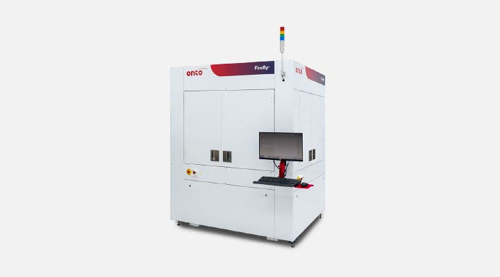
Dragonfly® G3 System
Highly configurable, automated, high speed 2D inspection and 3D metrology for inline process control in advanced packaging, specialty and front-end OQA.

From consumer products to industrial applications, augmented reality (AR)/mixed reality (MR) technology is one of the most innovative interactive technologies on the market today.

Sept 2 — Sept 4, 2026
Onto Innovation is a proud exhibitor at SEMICON Taiwan.
Explore how AI, high performance computing and big data are transforming technology, and learn how Onto Innovation supports these trends with advanced inspection, metrology, lithography and analytics.
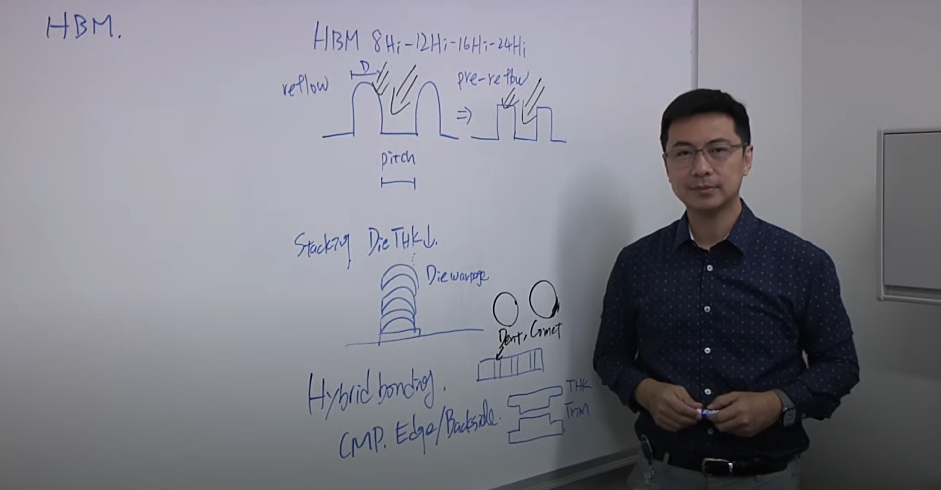
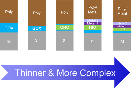
AI adoption is accelerating at an unprecedented pace, transforming industries from healthcare to finance. This explosive growth demands increasingly powerful semiconductor chips capable of processing massive datasets at lightning speed. However, producing these AI-optimized chips presents complex challenges in logic, memory, packaging and power.
Onto Innovation is at the forefront of enabling AI through advanced inspection, metrology and lithography systems. Our solutions support the fabrication of next-generation logic devices like Gate-All-Around (GAA) and FinFET architectures—essential for delivering the speed and efficiency AI workloads require. We also help enable high-bandwidth memory and stacked DRAM, which provide the essential memory capacity for large-scale AI models. Lithography plays a pivotal role in panel-level packaging by enabling the precise patterning of dense interconnects that connect logic, memory and chiplets.
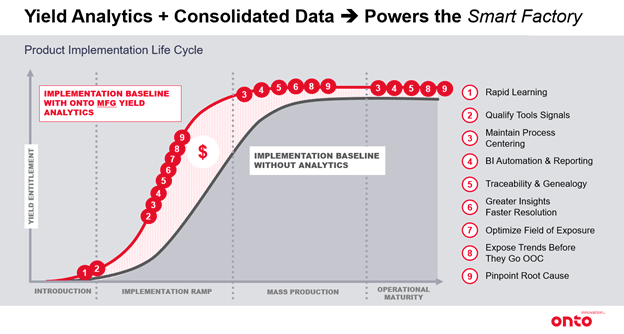
To further elevate AI chip manufacturing, our disruptive software solutions deliver predictive insights and actionable intelligence across nearly every process area, unlocking the full potential of your data.


High Performance Computing (HPC) is driving breakthroughs in AI, scientific research and data-intensive applications. As demand grows for faster, more efficient processing, the semiconductor industry is pushing the limits of memory, packaging and power technologies.
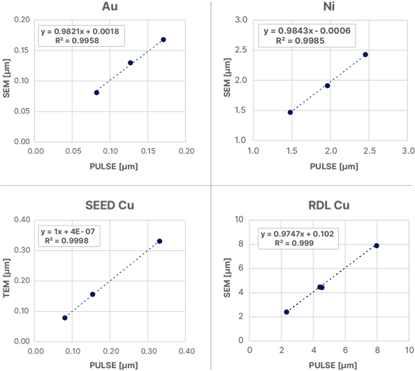
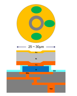
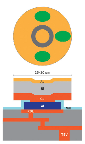
Onto Innovation plays a pivotal role in enabling HPC through advanced metrology and inspection solutions. We support cutting-edge memory technologies like high-bandwidth memory and next-gen stacked DRAM. Our deep expertise in advanced packaging enables precise 3D bump metrology, RDL printing and inspection—covering the majority of interconnects critical to HPC performance. We’re also leading innovation in panel-level packaging through collaborative development at our Packaging Application Center of Excellence, where we’re pioneering solutions to support next generation glass substrates.
Power efficiency is essential to HPC. Our process control technologies support compound semiconductors that drive high-performance systems.

Big data continues to reshape industries by enabling real-time analytics, AI, and smarter decision-making. This trend is fueled by the explosion of data from connected devices, cloud platforms and advanced applications. At the core of this evolution is the need for high-performance computing, driven by innovations in semiconductor technology.
Onto Innovation helps to accelerate this transformation by delivering metrology and inspection solutions that support the development of advanced logic and memory. Our technologies enable innovations like Gate-All-Around (GAA) and FinFET architectures in logic, as well as DRAM in memory, ensuring precision and reliability at nanoscale dimensions. We also enable compound semiconductor applications in power, analog, RF, laser and photonics.
Our technology extends to our powerful analytics software that connects data across tools, factories, and global supply chains—unlocking actionable insights and maximizing the value of your most critical asset: your data.


As your partner for innovative solutions, we’re always here for you.
Discover how our cutting-edge semiconductor solutions are engineered to meet your most complex challenges: delivering performance, reliability and innovation where it matters most.
"*" indicates required fields