
Dragonfly® G3 System
Automated high speed sub-micron 2D inspection and 3D inspection/metrology for inline process control of pattern defects in next generation technologies for advanced packaging, specialty and OQA.

If you’ve been following the evolution of advanced packaging, you know that the industry is pushing boundaries like never before. From high-performance computing to industry-upending AI devices, the demand for smaller, faster, and more powerful chips is driving innovation at every level.

The NSX 330 system offers advanced macro inspection for a wide range of defect sizes at high throughput, with optional 3D metrology integration.
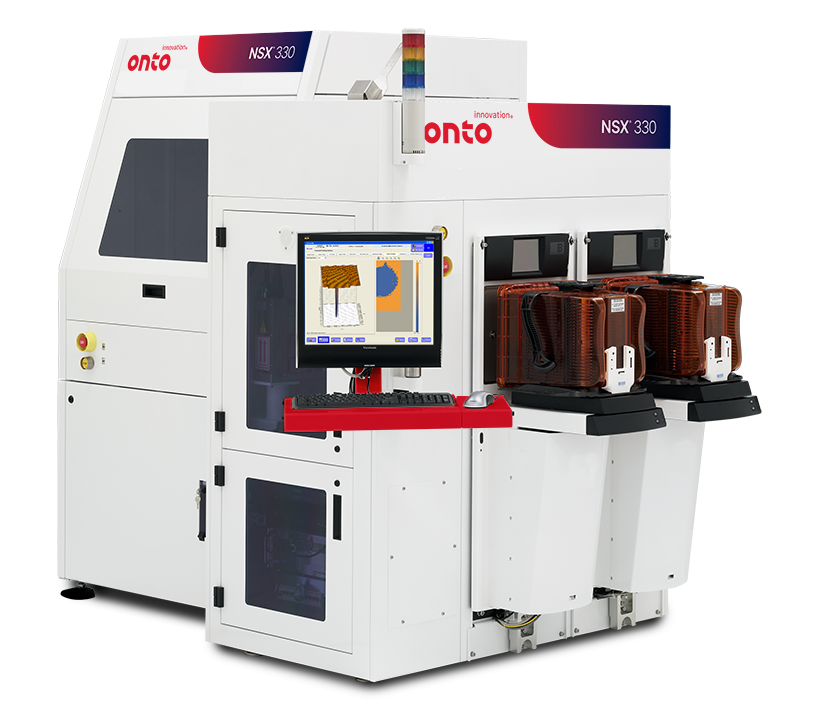
The NSX 330 system features robust platform technology with high-acceleration staging, high-speed multi-processor computing and flexible software. With over 1,000 installation worldwide, the NSX 330 System offers 2D inspection and metrology at high throughput and a broad portfolio of 3D sensors supporting critical advanced packaging applications. These include wafer-level metrology for micro bumps, RDL, kerf, overlay, and through silicon via (TSV) in a single wafer load.
Accommodating wafers from 100mm to 330mm, the system features a versatile objective turret, programmable light tower, and multiple dark field illumination modes. Additional features include resolution flexibility, unique handling solutions, and comprehensive software for recipe sharing and offline analysis. The NSX 330 system, with optional edge and backside inspection via the EB40 module, provides a comprehensive all-surface inspection solution packaging technology challenges.


As your partner for innovative solutions, we’re always here for you.
Discover how our cutting-edge semiconductor solutions are engineered to meet your most complex challenges: delivering performance, reliability and innovation where it matters most.
"*" indicates required fields
The Celero PL system is designed for subsurface defect inspection and classification for silicon carbide (SiC) and gallium nitride (GaN) based wafers and compound semiconductor materials.
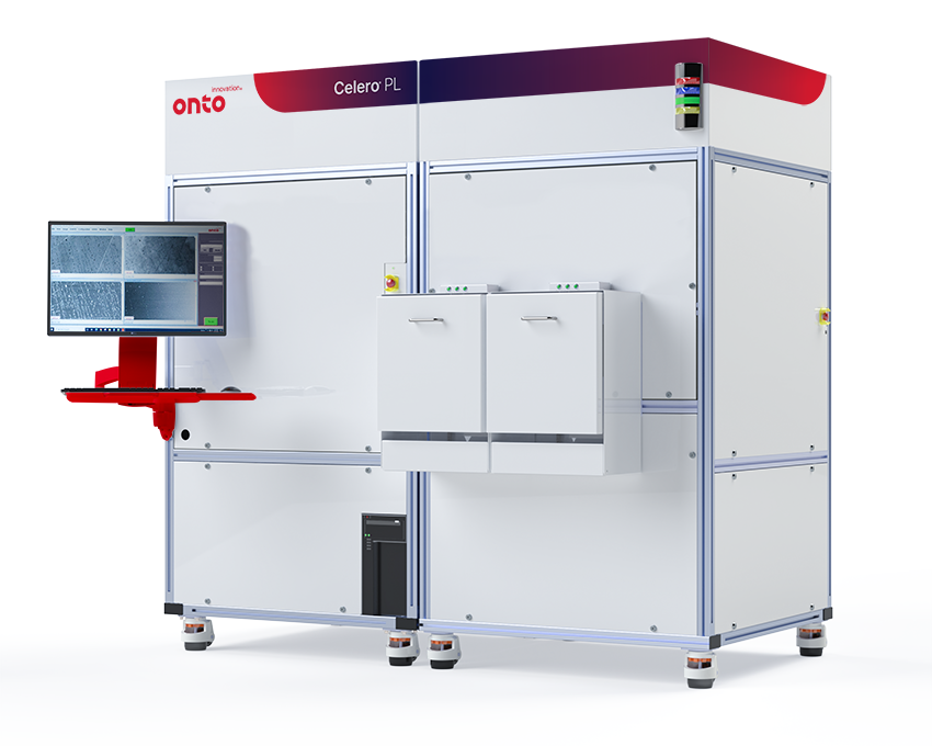
The Celero PL system utilizes a laser-based phase detection and imaging capability that leverages custom optics and image processing algorithms to enable best in class throughput and sensitivity for silicon carbide and gallium nitride-based materials on 100mm to 300mm wafer sizes. Leveraging multiple light sources and sensor channels, the system can detect, measure and image a broad variety of subsurface crystalline defects, associated with bulk wafers and epitaxial layers, surface particles, scratches, pits, surface contamination, stains, point or bulk wafer stress, voids/inclusions, including chips and cracks at the edge of the wafer.


As your partner for innovative solutions, we’re always here for you.
Discover how our cutting-edge semiconductor solutions are engineered to meet your most complex challenges: delivering performance, reliability and innovation where it matters most.
"*" indicates required fields
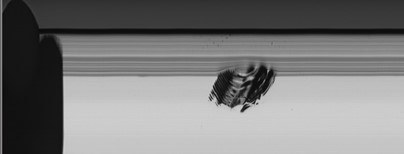
The Dragonfly G3 system is resetting the industry’s expectations for throughput, accuracy and reliability. Combining 2D and 3D technologies, the system detects yield-robbing defects and measures features critical for today’s front-end and packaging technologies.
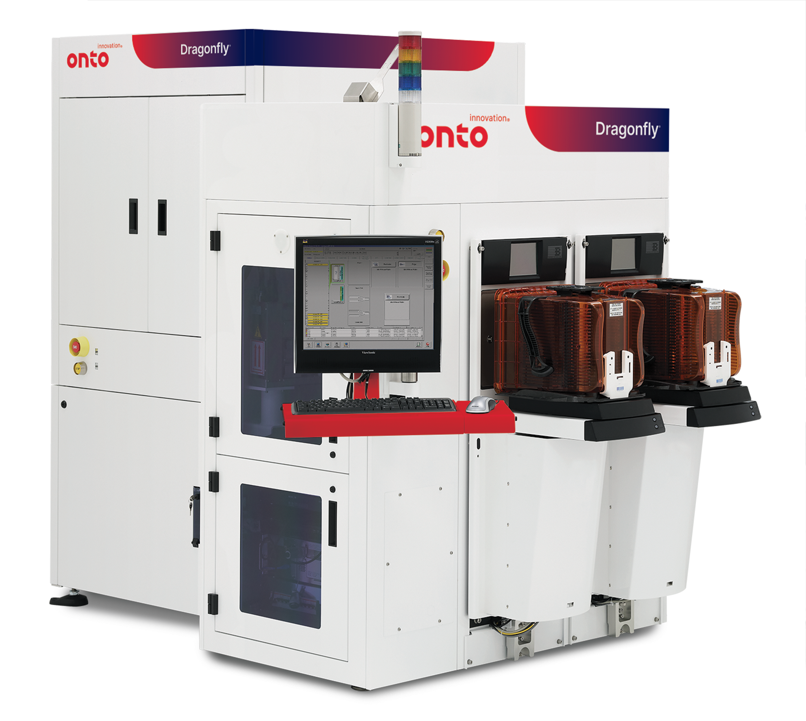
The Dragonfly G3 system utilizes line scan-based 2D imaging technology to provide fast, reliable inspection for sub-micron defects, meeting both current R&D and future production needs. It features multi-illumination channels, including brightfield/darkfield, high-speed IR for embedded defects and Clearfind® Technology for non-visual residue detection. For specialty markets like CMOS image sensors (CIS), it uses oblique angle illumination, sophisticated image processing and machine-learning algorithms to detect low contrast defects in the active pixel sensor area.
Optional 3D metrology sensors include the latest 3Di™ technology, delivering fast, precise bump height metrology. Discover Software visualizes the massive amounts of bump data, correlating process variations to improve yields. TrueADC software enables real time automatic classification of critical defects and reduces nuisance defects. The Dragonfly G3 system, with optional edge and backside inspection via the EB40 module, offers a comprehensive all-surface inspection solution for next generation technology challenges.
Hybrid bonding enables ultra-dense 3D memory interconnects with up to 1,000x more connections than microbumps. Achieving high yield requires stringent process control, including monitoring topography and detecting particles, cracks and voids. Measuring dishing in copper pads provides valuable insight into surface conditions. Together, these process control insights contribute to improved device reliability and performance.

As demand grows for high-performance computing (HPC) and AI-driven applications, manufacturers are turning to hybrid bonding to enable the ultra-dense 3D integration required for next-generation chip architectures. This advanced packaging technology presents significant process challenges. Surface preparation must be precisely controlled to eliminate particles, excess recess, and copper pad dishing, all of which can compromise bond quality. During pre-annealing, particle-induced gaps and wide bonding gaps can prevent proper wafer contact. Post-annealing, the formation of dielectric and metal voids introduces further risks to electrical performance and long-term reliability.

The Iris S system is a versatile platform solution for the advanced packaging and specialty market, supporting 150mm, 200mm and 300mm wafers. It provides thin and thick film, OCD and wafer bow and film stress measurements.

The IMPULSE V system helps to advance CMP processing with enhanced wavefront technology and AI-driven analytics, delivering over 2X precision improvement and faster solutions, crucial for next-gen semiconductor manufacturing demands.
The Dragonfly G3 system is resetting the industry’s expectations for throughput, accuracy and reliability. Combining 2D and 3D technologies, the system detects yield-robbing defects and measures features critical for today’s front-end and packaging technologies.

The Aspect System is a revolutionary in-line, non-destructive infrared optical critical dimension (IRCD) system measuring Z-dimension profiling of high aspect ratio structures to enable critical process control. It meets the needs of leading-edge customers with its high speed and process coverage.


As your partner for innovative solutions, we’re always here for you.
Discover how our cutting-edge semiconductor solutions are engineered to meet your most complex challenges: delivering performance, reliability and innovation where it matters most.
"*" indicates required fields
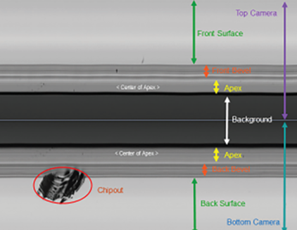
The NovusEdge G2 System offers fast, reliable edge, notch and backside inspection for 300mm unpatterned wafers, utilizing modular configurations.
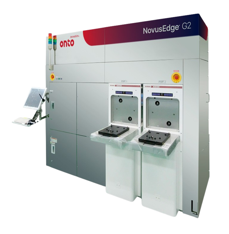
The NovusEdge G2 System provides high sensitivity inspection for the edge and backside of unpatterned wafers for current and advanced nodes. Configurable modules on the same automation platform increase throughput while maintaining a small footprint for improved cost of ownership. The edge-gripping handling solution for both automation platform and the inspection modules provide desired cleanliness required for manufacturing. Optional high-sensitivity notch inspection can be added. Defects are automatically classified and binned at run time to reduce manual review.
Designed as a multipurpose inspection and sorting system for end of line outgoing quality inspection of 300mm unpatterned wafers, the system identifies, inspects and sorts wafers according to recipes.
The NovusEdge G2 system offers higher sensitivity than the previous generation, with sub-micron resolution and increased throughput by over 15%. User interaction is simplified, and the new electrical design consumes less power.
As your partner for innovative solutions, we’re always here for you.
Discover how our cutting-edge semiconductor solutions are engineered to meet your most complex challenges: delivering performance, reliability and innovation where it matters most.
"*" indicates required fields
In the semiconductor industry, digital twins are the focus of a lot of attention, with substantial investments from industry players and governments alike. This year the European Union and the United States have pledged hundreds of millions of dollars in grants and funding opportunities, including the new CHIPS Digital Twin Manufacturing USA Institute. Ultimately, many people see great value in innovating, commercializing and scaling digital twin technology.
As with many trends, digital twins are the subject of speculation and fervor. Unfortunately, this enthusiasm can drive well intentioned users and organizations to choose solutions they don’t need – or spend too much time and money before arriving at reliable ones.
The concept of zero defect manufacturing has been around for decades, arising first in the aerospace and defense industry. Since then, this manufacturing approach has been adopted by the automotive industry, and it has only grown in importance as the sector transitions to electric vehicles. Given the role semiconductors play in today’s vehicles, and will play in the future, it is no surprise the industry has adopted a zero defect approach.
However, the quest for zero defect manufacturing goes well beyond the aerospace, defense, and automotive industries. Many companies that have started or are planning digital transformations are pursuing zero defect manufacturing. Accomplishing this requires using data from a wide range of sources, including materials, products, processes, factory subsystems, and equipment. When all of this data is properly integrated, and fabs are able to take complete advantage of the analytics from their monitoring systems, the goal of a zero defect manufacturing environment is achievable.
Before we go any further, we should get one thing out of the way: zero defect manufacturing does not promise zero defects. It is a commitment to properly identifying defects and sources, giving manufacturers the opportunity to detect dormant failures early on and make proactive corrections.