
Discover® Defect Software
Integrated defect management system that works seamlessly with Onto tools and your entire enterprise, bringing data together for greater visibility and cleaner operation.
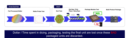
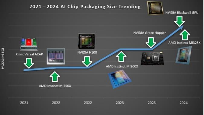
In a world where high-bandwidth memory, GPUs, and advanced AI packages are all the rage, it is easy to forget the important role specialty devices play.

May 5 — May 7, 2026
Onto Innovation is a proud exhibitor at SEMICON Southeast Asia.
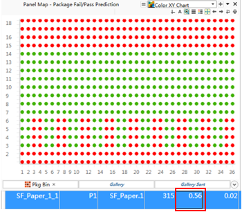
Discover Yield software is a complete yield management enterprise platform that combines parametric, defect and yield optimization with data mining and workflow development across all data sources from memory and design to assembly and packaging.
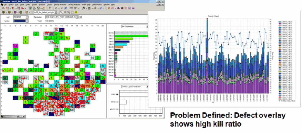
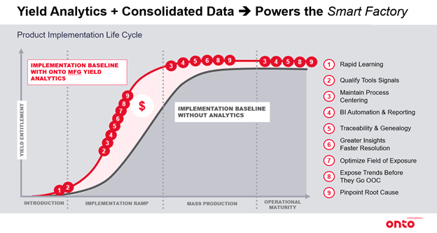
Discover Yield software helps reduce the time it takes to find root causes of yield excursions and enables manufacturers to broaden their analysis scope for better yield management.
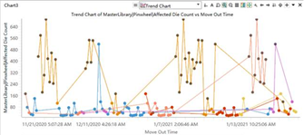
The software includes data acquisition and integration, a development environment through workflow and scripting, and specialized analysis algorithms to identify domain-specific issues, such as data mining, spatial anomalies, wafer processing sequence problems, commonality of effects, system and random yield loss, chamber matching, tool events, traceability and more. In addition, Discover Yield software provides distinct tools – principal components and multivariate analysis of variance (MANOVA) – that allow systematic, simultaneous examination of multiple variables. Discover Yield software’s database architecture for genealogy uniquely supports value chain predictive analytics.
Improving baseline yield with analytics


As your partner for innovative solutions, we’re always here for you.
Discover how our cutting-edge semiconductor solutions are engineered to meet your most complex challenges: delivering performance, reliability and innovation where it matters most.
"*" indicates required fields
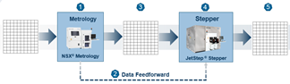
An advanced feed-forward lithography software solution for fan-out panel level packaging that enhances yield and throughput by correcting die placement errors through external measurements, predictive analytics and adaptive shot control.
StepFAST® software is Onto Innovation’s advanced lithography software solution tailored for fan-out panel-level packaging, where die placement errors and material instability can significantly impact yield and productivity. StepFAST® software uses a feed-forward adaptive shot approach, integrating high-speed die placement measurements from the Firefly® system and applying real-time corrections to every shot of the JetStep® lithography tool. This external measurement strategy doubles throughput compared to traditional on-tool (self-metrology) methods. The software also incorporates predictive yield analysis, enabling dynamic adjustment of exposure field sizes to balance throughput and overlay accuracy. By automating reticle selection and optimizing field coverage, StepFAST® software ensures efficient panel exposure while minimizing registration errors—from ±50µm down to under ±3µm. With advanced analytics, StepFAST® software transforms lithography into a flexible, high-efficiency process, delivering substantial improvements in yield, throughput, and cost of ownership for panel-level packaging applications.
Die shift on reconstituted panels can significantly impact both productivity and yield. To address this challenge, we use a parallel die placement measurement process and advanced analytics to provide a means to balance productivity against yield. Our integrated lithography cell, featuring Firefly inspection, StepFAST software, and JetStep Lithography, delivers industry-leading throughput and yield for fan-out panel level packaging.
It is well understood that advanced packaging applications require high performance, low cost, increased functionality and improved reliability that 2.5D and 3D packaging solutions provide. Fan-out panel-level packaging (FOPLP) is one of the technologies that has the potential to meet these packaging requirements.
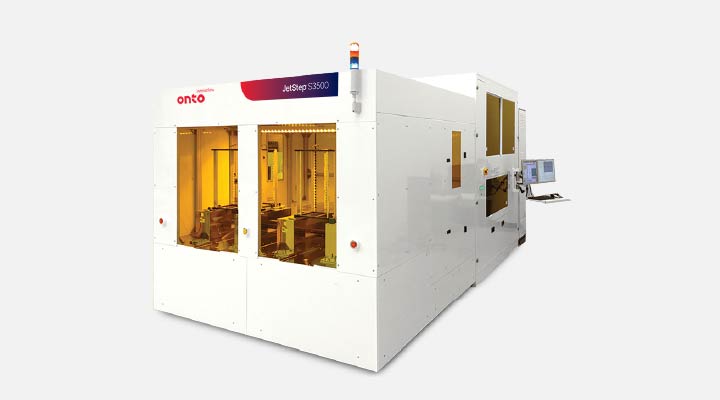
The JetStep S3500 system is designed to provide OSATS with a high-volume manufacturing advanced packaging lithography solution. For substrates up to 720mm x 600mm, it supports fan-out panel level packaging.
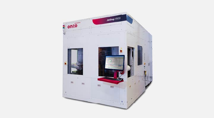
The JetStep X500 system is designed to provide AICS and OSAT manufacturers with a high-volume manufacturing lithography solution for heterogeneous integration. The JetStep X500 system exposes panel-type substrates made of CCL, FR4, composite, glass or other materials.
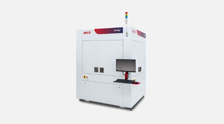
The Firefly G3 system provides automated inspection and 3D metrology for advanced IC substrates and panel level packaging, delivering high resolution and productivity for demanding applications like high-performance computing (HPC), artificial intelligence (AI), cloud computing and machine/deep learning.

An advanced feed-forward lithography software solution for fan-out panel level packaging that enhances yield and throughput by correcting die placement errors through external measurements, predictive analytics and adaptive shot control.
As your partner for innovative solutions, we’re always here for you.
Discover how our cutting-edge semiconductor solutions are engineered to meet your most complex challenges: delivering performance, reliability and innovation where it matters most.
"*" indicates required fields
The JetStep X500 system is designed to provide AICS and OSAT manufacturers with a high-volume manufacturing lithography solution for heterogeneous integration. The JetStep X500 system exposes panel-type substrates made of CCL, FR4, composite, glass or other materials.
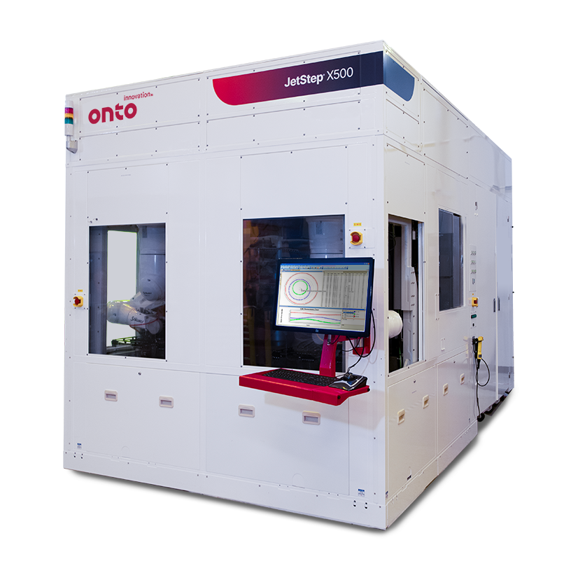
The JetStep X500 panel lithography system is optimized for high volume manufacturing of high-end AICS and other advanced packaging panel applications. As we approach the limits of Moore’s law, the JetStep X500 system addresses the need for extremely large packages integrating multi-node chips, or “chiplets,” enhancing functionality, speed, I/O count and reducing power consumption for server farms, AI, and mobile applications. The JetStep X500 system features the industry’s largest exposure field , fine line RDL resolution with large depth of focus (DOF), excellent overlay accuracy, and automatic magnification compensation with independent x and y magnification adjustment. The JetStep X500 system handles a large range of substrate thicknesses with high levels of warp, offering unique imaging parameter control to compensate for panel distortion. Additionally, it can run highly warped substrates with an edge clamping option and provides real-time autofocus at every exposure site to compensate for challenging topography.


Die shift on reconstituted panels can significantly impact both productivity and yield. To address this challenge, we use a parallel die placement measurement process and advanced analytics to provide a means to balance productivity against yield. Our integrated lithography cell, featuring Firefly inspection, StepFAST software, and JetStep Lithography, delivers industry-leading throughput and yield for fan-out panel level packaging.
It is well understood that advanced packaging applications require high performance, low cost, increased functionality and improved reliability that 2.5D and 3D packaging solutions provide. Fan-out panel-level packaging (FOPLP) is one of the technologies that has the potential to meet these packaging requirements.
The JetStep S3500 system is designed to provide OSATS with a high-volume manufacturing advanced packaging lithography solution. For substrates up to 720mm x 600mm, it supports fan-out panel level packaging.
The JetStep X500 system is designed to provide AICS and OSAT manufacturers with a high-volume manufacturing lithography solution for heterogeneous integration. The JetStep X500 system exposes panel-type substrates made of CCL, FR4, composite, glass or other materials.
The Firefly G3 system provides automated inspection and 3D metrology for advanced IC substrates and panel level packaging, delivering high resolution and productivity for demanding applications like high-performance computing (HPC), artificial intelligence (AI), cloud computing and machine/deep learning.
An advanced feed-forward lithography software solution for fan-out panel level packaging that enhances yield and throughput by correcting die placement errors through external measurements, predictive analytics and adaptive shot control.
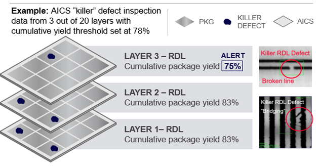
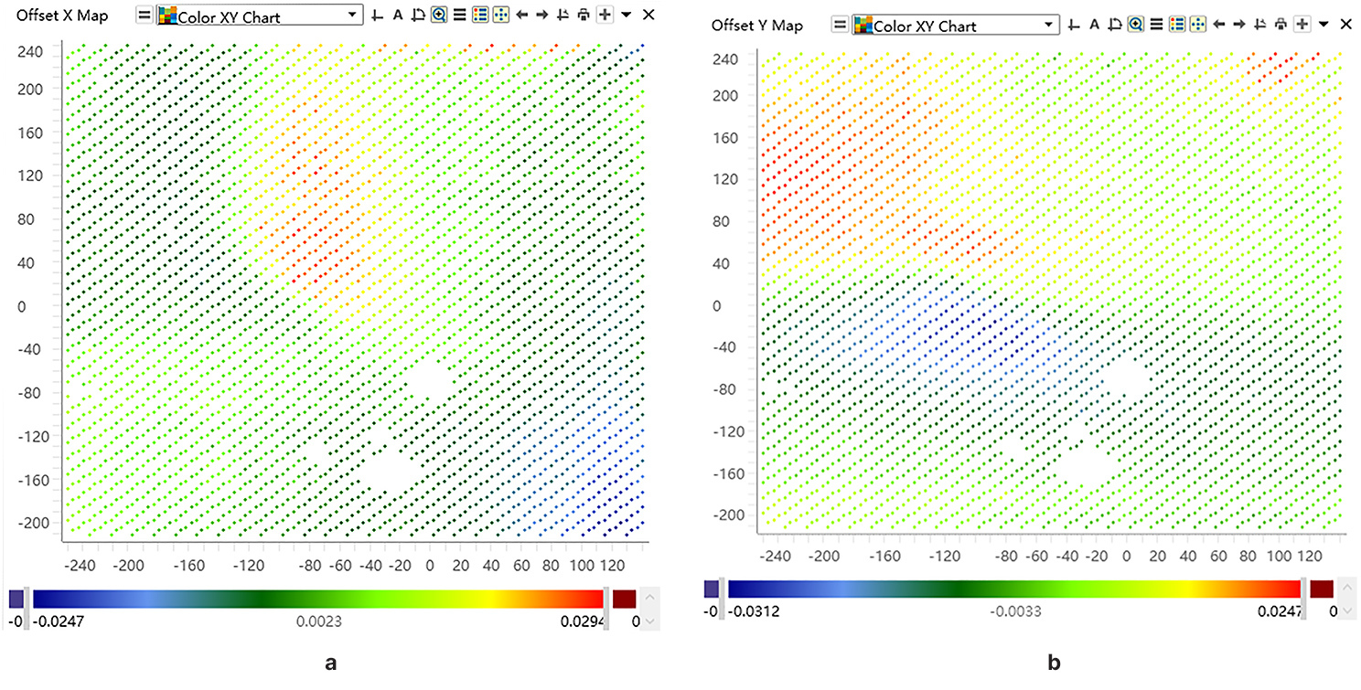
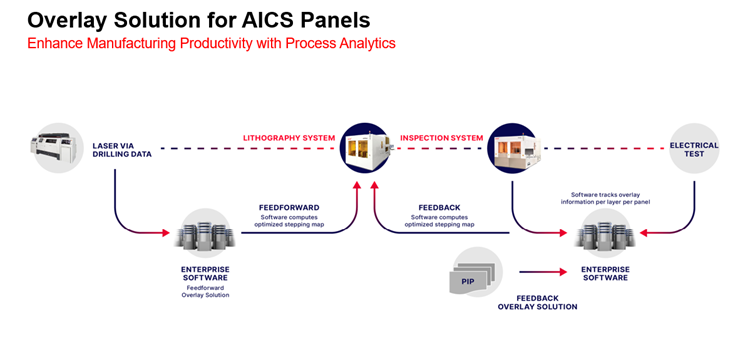
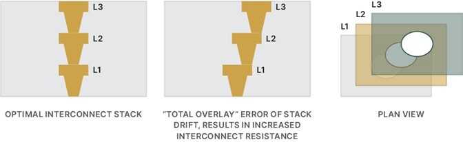
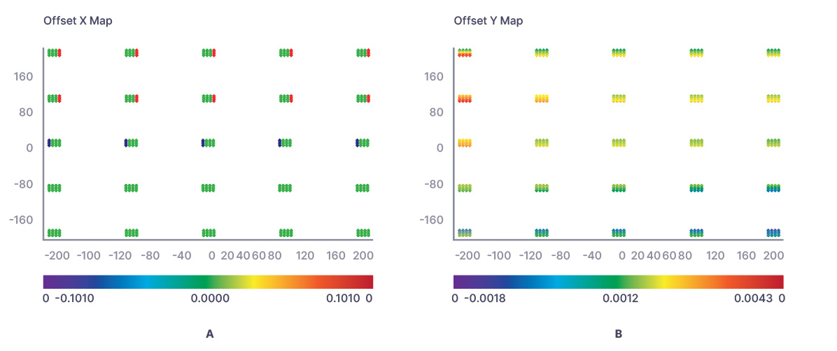
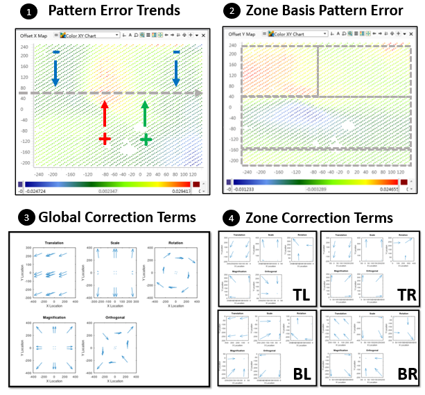
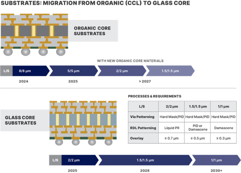
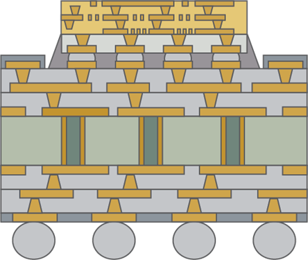
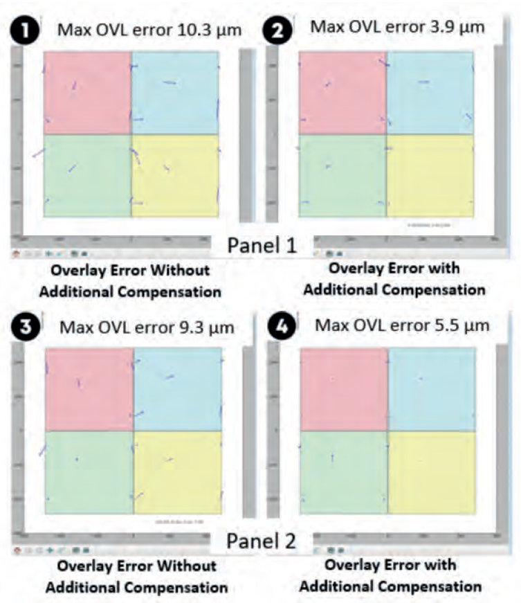
During the processing of organic (CCL) advanced IC substrates (AICS) the substrates become distorted which impacts the overlay of Via to RDL pad structures. To solve this problem, the stepper must adjust the alignment solution to match the previous layer’s distortion by measuring the overlay. Proprietary software provides the user with the ability to adjust each zone of the AICS with independent offsets.
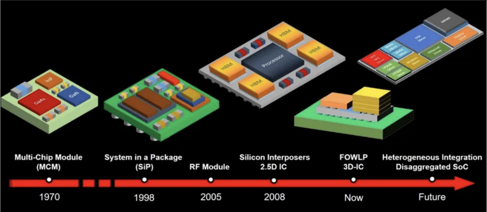
The growing demand for heterogeneous integration is driven by the 5G market. This includes smartphones, data centers, servers, high-performance computing (HPC), artificial intelligence (AI) and internet of things (IoT) applications. Next generation packaging technologies require tighter overlay to accommodate larger package sizes with fine-pitch chip interconnects on large-format flexible panels.
Designed for advanced IC substrates (AICS), it incorporates a large field exposure area with a large depth of focus. Proprietary software enables independent zone offset adjustments across the AICS.
The Firefly G3 system provides automated inspection and 3D metrology for advanced IC substrates and panel level packaging, delivering high resolution and productivity for demanding applications like high-performance computing (HPC), artificial intelligence (AI), cloud computing and machine/deep learning.


As your partner for innovative solutions, we’re always here for you.
Discover how our cutting-edge semiconductor solutions are engineered to meet your most complex challenges: delivering performance, reliability and innovation where it matters most.
"*" indicates required fields
The JetStep S3500 system is designed to provide OSATS with a high-volume manufacturing advanced packaging lithography solution. For substrates up to 650mm x 650mm, it supports fan-out panel level packaging.
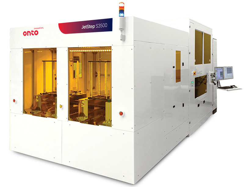
The JetStep S3500 panel lithography system is specifically designed for advanced packaging panel production. As fan-out packages increase in size and complexity, requiring panel substrates instead of wafers, the JetStep S3500 system addresses these challenges with advanced features. It handles die shift caused by placement accuracy errors, CTE mismatch and panel warpage. The system incorporates a large exposure field (59.4 x 59.4mm) with resolution capability to 2/2 L/S and options for increased resolution to 1/1. In addition, it supports multiple exposure wavelengths, ideal for process development with new photosensitive polymers. Application-specific options include warped panel handling, “on-the-fly” optical focus, and die shift correction (StepFAST™ Solution), helping to ensure precise and reliable panel-level packaging.
Die shift on reconstituted panels can significantly impact both productivity and yield. To address this challenge, we use a parallel die placement measurement process and advanced analytics to provide a means to balance productivity against yield. Our integrated lithography cell, featuring Firefly inspection, StepFAST software, and JetStep Lithography, delivers industry-leading throughput and yield for fan-out panel level packaging.
It is well understood that advanced packaging applications require high performance, low cost, increased functionality and improved reliability that 2.5D and 3D packaging solutions provide. Fan-out panel-level packaging (FOPLP) is one of the technologies that has the potential to meet these packaging requirements.
The JetStep S3500 system is designed to provide OSATS with a high-volume manufacturing advanced packaging lithography solution. For substrates up to 720mm x 600mm, it supports fan-out panel level packaging.
The JetStep X500 system is designed to provide AICS and OSAT manufacturers with a high-volume manufacturing lithography solution for heterogeneous integration. The JetStep X500 system exposes panel-type substrates made of CCL, FR4, composite, glass or other materials.
The Firefly G3 system provides automated inspection and 3D metrology for advanced IC substrates and panel level packaging, delivering high resolution and productivity for demanding applications like high-performance computing (HPC), artificial intelligence (AI), cloud computing and machine/deep learning.
An advanced feed-forward lithography software solution for fan-out panel level packaging that enhances yield and throughput by correcting die placement errors through external measurements, predictive analytics and adaptive shot control.
As your partner for innovative solutions, we’re always here for you.
Discover how our cutting-edge semiconductor solutions are engineered to meet your most complex challenges: delivering performance, reliability and innovation where it matters most.
"*" indicates required fields
Discover AI software leverages high-quality data input to provide valuable insights into processes and actionable predictions for process, yield and efficiency improvements through integration with the Discover data platform.
Discover AI software is a disruptive technology that reshapes the way we approach manufacturing line control and yield analysis. It leverages the latest in machine learning and artificial intelligence to identify actionable improvements and connections in data that a human could not. The software’s optimization engine adds a powerful machine learning analytical method to an already sophisticated toolbox of process improvement applications.
By analyzing any set of conceivable inputs and outputs, Discover AI software identifies relationships and interactions that lead to positive operational changes. Easily understood visuals empower even casual users to understand what is important before making adjustments.
Discover AI software evaluates multiple models and suggests the optimal one for the data. Using machine learning, it examines interactions between in-process inputs and results for any semiconductor product family and recommends changes to in-process targets. Licensed as a service, it enables users to leverage an on-demand infrastructure to apply easily understood workflows for complex analytics without the overhead.
As your partner for innovative solutions, we’re always here for you.
Discover how our cutting-edge semiconductor solutions are engineered to meet your most complex challenges: delivering performance, reliability and innovation where it matters most.
"*" indicates required fields
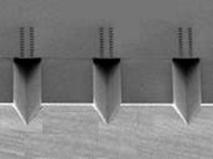
The IVS 380 System delivers overlay, CD and z-height metrology for advanced packaging, power, compound semi and MEMS, offering world class performance and flexibility to accommodate substrates of different sizes and thickness without hardware changes.
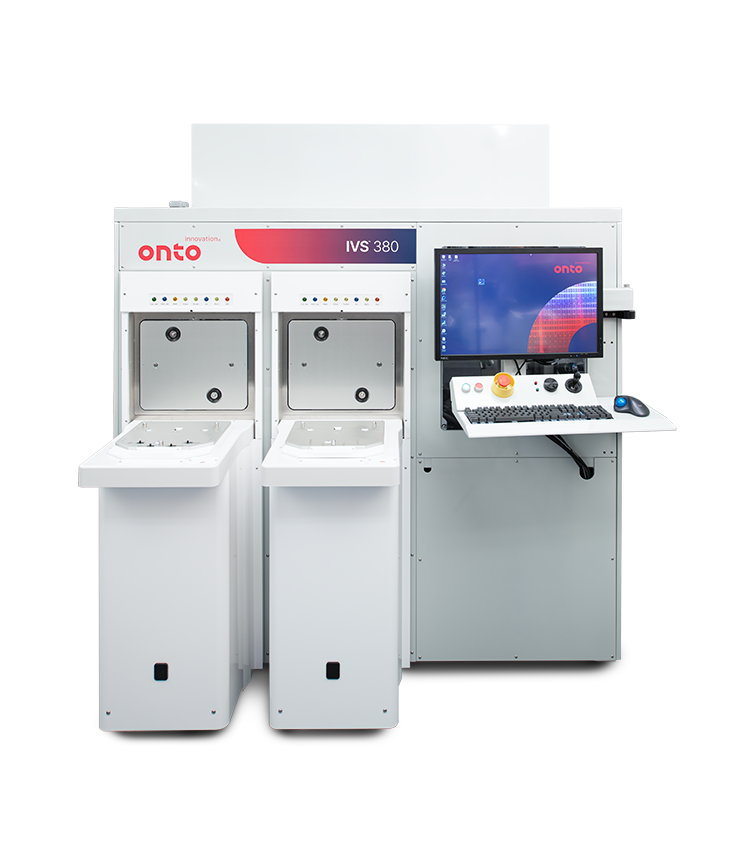
The IVS 380 is an optical overlay, CD & z-height metrology system designed for high volume manufacturing, with SMIF (200mm substrate) or FOUP (300mm substrate) load ports compatibility. It handles various substrates for advanced packaging, including Si, glass and CCL, and accommodates sizes of 200mm and 300mm.
Building on the IVS family’s 40 years of experience in CMOS, MEMS and compound semiconductor applications, the IVS 380 system possesses the versatility to tackle overlay, CD and z-height measurements for diverse substrates and layers. It measures critical dimensions in the xy plane and the vertical z-heights of features like RDL metal lines, posts and bumps. The optics enable focus on mostly transparent materials such as photoresists and rough surfaces such as electroplated copper.
Enter your information below and we’ll send you a unique passcode to view our IVS 3D Demo.
As your partner for innovative solutions, we’re always here for you.
Discover how our cutting-edge semiconductor solutions are engineered to meet your most complex challenges: delivering performance, reliability and innovation where it matters most.
"*" indicates required fields