

As semiconductor manufacturers push the boundaries of performance and functionality—driven by high-performance computing and AI applications—chemical mechanical planarization (CMP) processes increase in intensity complexity.
New logic transistor designs, 3D NAND stacking, and DRAM integration introduce more CMP layers and tighter process windows. Traditional metrology approaches struggle to keep pace, especially with the need for high sampling rates, multiple control zones, and improved signal-to-noise ratios.

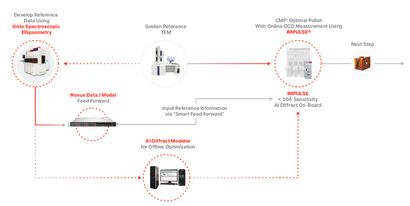
Onto Innovation’s Intelligent Line Monitoring & Control with Integrated Metrology offers a transformative approach to CMP process control.
By leveraging data feedforward from standalone metrology tools to integrated metrology systems, this solution enables real-time, AI-driven process optimization.
At the heart of this solution is the IMPULSE® V system, an advanced integrated metrology platform that connects with standalone tools like the Atlas® system and utilizes Ai Diffract™ modeling software.
This ecosystem enables the creation of hybrid reference models—combining standalone data and limited TEM measurements—to drive high-precision, high-throughput results.
Key Benefits
Accelerated Time to Solution: Feedforward of secondary parameters from standalone tools into IMPULSE system recipes enables faster model convergence and process tuning.
Improved Throughput: Skipping pre-measurements at the integrated metrology stage saves time without compromising accuracy
Reduced Cost and TEM Dependency: Hybrid reference modeling minimizes the need for extensive TEM data, reducing both cost and development time.
Enhanced Process Control: AI-driven analytics and model-based feedback improve excursion detection and process stability, leading to better Cpk performance.
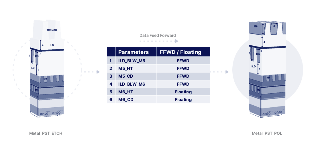
In-Fab Use Case
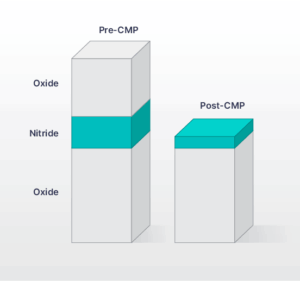
MX PST-POL Full Loop
In a production environment, Onto Innovation demonstrated the power of feedforward data integration by correlating oxide loss measurements across standalone and integrated metrology tools. By feeding forward key parameters, the solution eliminated the need for redundant pre-measurements and improved correlation to reference data—delivering both time savings and enhanced process control.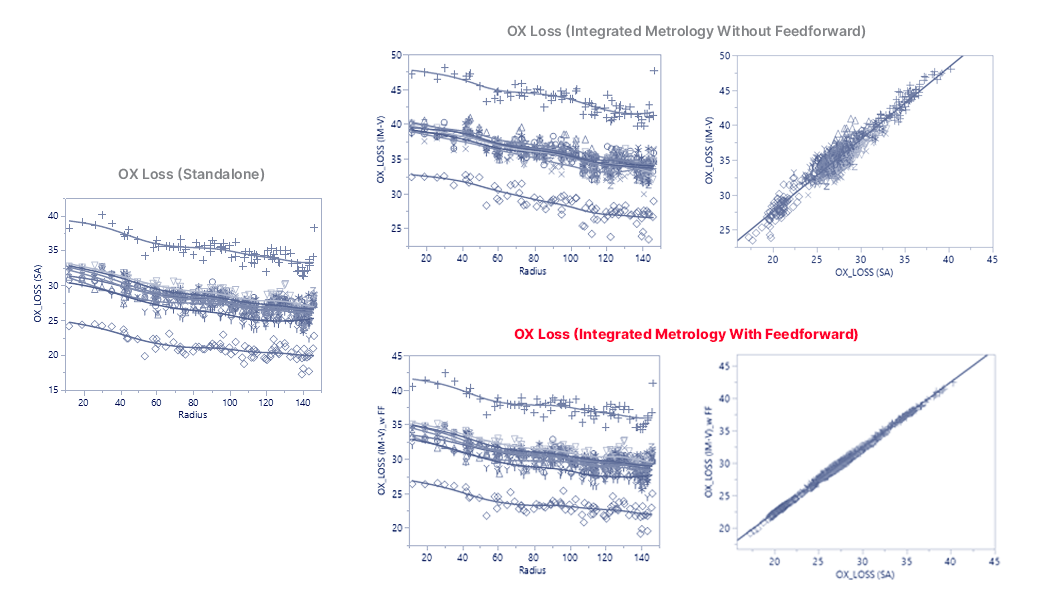

You Have a Challenge? Let’s talk.
We’d love to connect with you.
Looking to learn more about our innovative solutions and capabilities? Our team of experts is ready to assist you. Reach out today and let’s starts a conversation about how we can help you achieve your goals.
Let’s Talk
"*" indicates required fields
As artificial intelligence (AI), high-performance computing (HPC), and advanced graphics processing continue to push the limits of memory throughput, the demand for high-bandwidth memory (HBM) has surged. These applications require faster access to massive datasets, driving the need for memory solutions that can deliver both speed and density without compromising power efficiency. HBM addresses this by stacking memory dies vertically and connecting them with ultra-fast interconnects. However, as data rates climb, traditional bump technologies—long relied upon as the primary interconnect method—are reaching their physical and performance limits.
Today, we stand at a pivotal moment in HBM interconnect technology. Hybrid bonding has emerged as one of the most talked-about technologies in advanced packaging. Promising finer pitches and superior electrical performance, hybrid bonding is generating excitement for its potential in high-performance applications. On the other hand, innovations in bump scaling are making bumps increasingly viable for a broad range of applications, beyond legacy and cost-sensitive applications. Despite these advancements, scaling bump pitch beyond 10μm and toward 2μm presents significant challenges. Maintaining uniformity and controlling bump height variation becomes more difficult, impacting yield and reliability. Meanwhile, taller HBM stacks, from 8-high to 24-high, require thinner dies, increasing the risk of die warpage and cracks during dicing.
Hybrid bonding is not without its challenges, too. At this scale, direct bonding demands plating uniformity and surface cleanliness to ensure reliable interconnects. In this article, we will examine the challenges facing bump and hybrid bonding technologies, the solutions these two technologies enable, and how they stack up compared to each other. We also will highlight how manufacturability, reliability, and process control evolve as pitches shrink and stack heights increase. To start with, we focus our attention on bumps, and then move on to hybrid bonding.
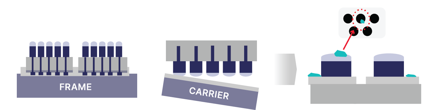
Bump metrology evolution
Microbumps play a critical role in enabling vertically-stacked HBM structures by serving as interconnects between dies, and dies to interposers or substrates. These bumps need to be uniform in height, properly aligned, and defect free (Figure 1).

Figure 1. Interconnect challenges in microbump and hybrid bonding technologies.
Inconsistent bump height in HBM can result from plating nonuniformity and process variability, and it negatively affects yield, reliability, and performance. Meanwhile, poor coplanarity can lead to mechanical stress, interconnect fatigue, or thermal cycling failures, while inconsistent contact can degrade signal integrity and power delivery. Misalignment during flip-chip bonding can result in open or short circuits. Given the breadth of these challenges, manufacturers should focus on identifying issues after the plating step and before the reflow step. After all, if you have a plating problem but move onto reflow, it will be too late to fix the problem.
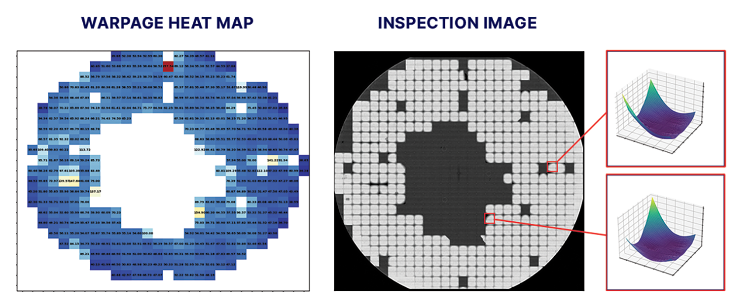
With the number of layers in an HBM stack continuing to rise, addressing die warpage becomes even more essential (Figure 2). First of all, die warpage significantly compromises stack alignment and bonding quality. This is especially critical given the extremely tight tolerances of HBM. In addition, warpage can also result in voids, opens, and a host of other issues leading to electrical failures, mechanical stress and cracking, yield loss, and thermal performance degradation, resulting in overheating and reduced performance. Meanwhile, organic residue can result in surface contamination, voids and delamination, oxidation and corrosion, and diminished yield and reliability.
Properly identifying cracks and alignment errors in bumps poses another challenge (Figure 3). Cracks often occur during the dicing and backside grinding process and can break the electrical path, leading to open circuits. They often propagate due to thermal cycling, especially in materials with different coefficients of thermal expansion (CTE), weakening the bump structure. Even if initially functional, cracked bumps are prone to failure under thermal or mechanical stress during operation.
Misalignment of dies is another problem. It is often caused during the pick and place step due to the lack of backside patterns. This lack of patterning makes it difficult to tell if overlay is accurate—this is something with which automated optical inspection systems struggle.
Rise of hybrid bonding
The key reason hybrid bonding has emerged as a new technology for HBM is simple: improved interconnect density and smaller package sizes. To begin with, hybrid bonding enables finer interconnect pitches, less than 10μm, allowing for more I/O terminals in a smaller area. This increased density translates directly into higher bandwidth and improved overall performance.
Traditional bump-based stacking introduces gaps of about 30μm between dies. Hybrid bonding offers direct Cu-to-Cu connections, thereby achieving near-zero spacing between dies, significantly reducing overall package thickness and offering lower resistance and better thermal conductivity than bump-based methods. This improves signal integrity, reduces power consumption, and enhances heat dissipation, all of which are critical for HBM.
Finally, hybrid bonding supports several configurations: wafer-to-wafer, die-to-wafer, and die-to-die, offering flexibility in manufacturing and integration. This adaptability is vital for scaling HBM technologies across different applications and performance tiers.
With our introduction to bumps and hybrid bonding complete, we now turn to a comparative discussion of these two technologies, building on earlier points and exploring new ones.
Bump vs. hybrid bonding
Bumps have several advantages over hybrid bonding. As a mature technology, they are widely used and well understood in the industry, are compatible with existing flip-chip and underfill processes, and are scalable for moderate density. The cost of bump technologies is lower than hybrid bonding technologies. Bumps, however, have a number of disadvantages compared to hybrid bonding. The most significant of which are the pitch limitations of bump technologies, which struggle at pitches below 10µm due to challenges in plating uniformity and solder reflow. Bumps also require underfill, which can introduce stress and complicate thermal management.
Despite the limitations noted above, bump technology continues to evolve. Leading suppliers of bump plating systems project a continued downscaling of bump dimensions, with diameters decreasing to the 4µm-5µm range and heights dropping as low as 1µm to 2µm. At a 10µm pitch, the lateral footprint remains sufficient to support the high-density I/O requirements of advanced memory architectures. Concurrently, the reduced bump height enables vertical integration of up to 16 stacked HBM dies within the 775µm maximum package height defined by Joint Electron Device Engineering Council (JEDEC) standards. Consequently, bump interconnects remain a viable and scalable solution for next-generation HBM, and major manufacturers are maintaining substantial R&D investments in bump technology.
Hybrid bonding, while promising, presents its own set of challenges. In addition to being more expensive than traditional bump technologies, hybrid bonding may require manufacturers switching from bump technology to purchase new equipment and adopt new process flows. In addition, hybrid bonding is especially sensitive to particles and organic residues; for example, even 1µm particles can cause defects. Such residues can prevent proper contact, trap gases or moisture, and lead to void formation during bonding. These voids can cause delamination or incomplete bonding, reducing mechanical integrity and electrical continuity.
Interconnect solutions
Process control for hybrid bonding is challenging, but these obstacles can be addressed by employing a suite of advanced metrology and inspection technologies, as well as analytic software solutions.
High-speed, sub-micron inspection can be used to detect surface anomalies such as particles, residues, and backside and edge defects (Figure 4). This ensures that bonding surfaces are clean and defect-free before the bonding process begins. As for overlay misalignment, the capability to measure wafer topography and alignment with sub-micron precision enables accurate die placement and reduces the risk of misalignment during bonding. As for voids, a non-contact, immersion-free acoustic metrology technology capable of detecting voids down to 1µm is effective at identifying bonding defects that could lead to electrical or thermal failures. Furthermore, a sub-micron inspection system can be used to detect defects like cracks and delamination caused by thermal or mechanical stress.
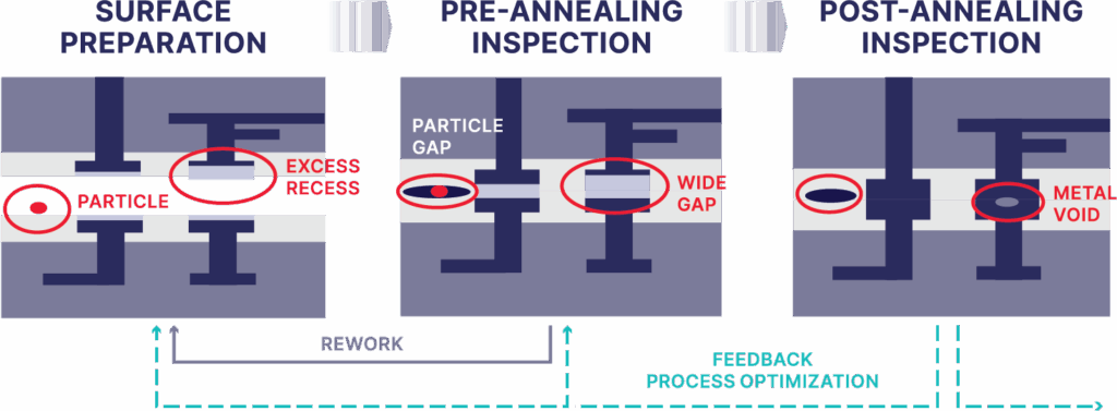
Figure 4: Hybrid bonding metrology and inspection challenges.
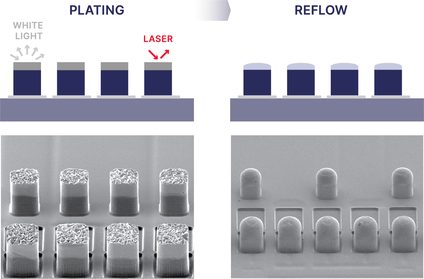
In the case of bump-based interconnects, the ability to measure Cu-to-Cu bump height down to 1.5μm will be key. However, several of today’s technologies employ white light illumination technologies that are unable to properly identify defects on these exceptionally small Cu pillars before reflow (Figure 5). After reflow, the bump shape is very clean and very smooth; but before reflow and after plating, the Cu is very rough. Typically, when white light hits a very rough surface, the light randomly scatters. However, an inspection system that uses a coherent wavelength laser technology can overcome this challenge.
In addition to the points noted above, an integrated system using analytical software can be used to detect errors and provide real-time defect analysis and statistical process control. Software can be used to provide in-line process control insights about defects and offer actionable corrections and is capable of handling millions of bumps per wafer, with each bump generating multiple data points. This integration helps manufacturers trace contamination sources and optimize cleaning steps, improving bonding reliability.
Summary
New technologies are actively being adopted for interconnect control in HBM. In the case of bump process control, the sector is moving toward smaller dimensions, 12µm to 4µm in high-volume manufacturing and below 2µm in R&D. Meanwhile, hybrid bonding is gaining traction due to its ability to support higher interconnect density and performance. This shift is driving the adoption of advanced inspection and metrology techniques, including an opto-acoustic void detection technology capable of detecting voids down to 1µm—a critical point for yield in HBM production.
Foundries are integrating bump inspection and metrology tools into their advanced packaging lines, especially for custom HBM and logic solutions. At the same time, hybrid bonding adoption is accelerating, particularly in the case of chiplet-based and heterogeneous integration strategies.
This year, R&D is expected to push microbump pitch to 6µm and hybrid bonding density to 60 interconnects/mm². In the coming years, microbump pitch may scale down to 3µm, while hybrid bonding density could reach 100 interconnects/mm². Long term, hybrid bonding is projected to become a mainstream interconnect technology, surpassing microbumps in many advanced applications, with densities reaching 150 interconnects/mm² and microbump pitch shrinking to 1.5µm.
As it stands today, there is no single solution for all HBM use cases. Instead, manufacturers may adopt an approach leveraging both bump and hybrid bonding, supported by a comprehensive process control strategy that integrates metrology, inspection, and advanced analytics.
Biographies
Damon Tsai is the Senior Director of Product Marketing, Inspection, at Onto Innovation, Milpitas, California. He joined the company in 2018 and has extensive experience in inspection and metrology, with a specialized focus on semiconductor FEOL, advanced packaging, OSAT, and specialty markets like RF, Power, and CIS.
Woo Young Han is Product Marketing Director, Inspection, at Onto Innovation, Richardson, Texas. He joined Onto Innovation in 2000 and holds an Electrical Engineering degree from the University of Toronto.
You Have a Challenge? Let’s talk.
We’d love to connect with you.
Looking to learn more about our innovative solutions and capabilities? Our team of experts is ready to assist you. Reach out today and let’s starts a conversation about how we can help you achieve your goals.
Let’s Talk
"*" indicates required fields
At some point in our lives, we have dropped a drinking glass or knocked over a glass-blown knickknack, only to watch it hit the floor and shatter into pieces. We learn from any early age that glass is fragile. But if glass is so fragile, why are manufacturers adopting glass core substrates?
Good question. And one that comes with a ready answer.
Glass is able to meet the new, denser line-space specifications—1.5µm and below—for interconnects that advanced logic nodes and advanced packages require. Two, glass core is better suited for large package sizes than organic substrates (Figure 1). And contrary to what those outside the semiconductor industry may think, glass substrate offers superior mechanical strength compared to its organic counterpart.
As it stands today, organic substrates will remain viable for advanced packages, but in the near future glass substrates might emerge as the preferred substrate for high-performance applications (Figure 1).
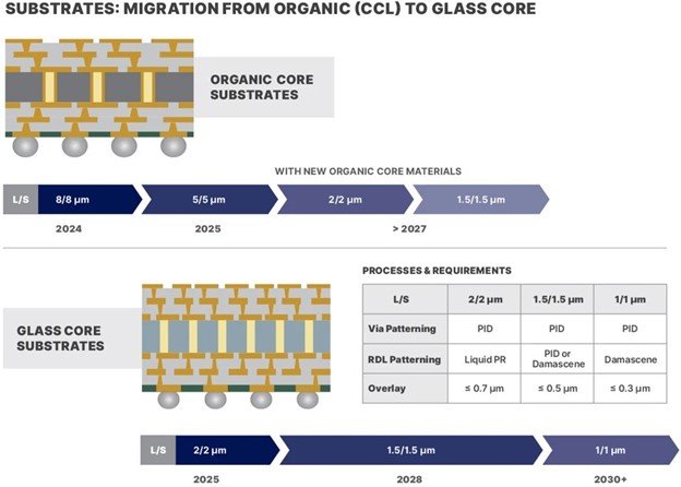
Figure 1: Roadmap for organic and glass core substrates
Through glass vias (TGVs) are the critical vertical electrical connections that pass through a glass substrate, and they require ultra-precise processing. Unfortunately, each step opens the process to a host of potential defects. Cracks, in particular, are problematic. A small crack early in the process has the potential to grow into a much larger, “killer” defect later in the manufacturing process that affects the performance and reliability of the end product.
These challenges are not limited to cracks, however. The position accuracy of TGVs is vital to ensure reliable electrical connections between the front and back of the glass substrate. Even slight misalignments can lead to signal integrity issues or device failure. In addition, the shape and size of the vias are another area of concern; as a result, the critical dimensions (CD) of these vias must be tightly controlled. The relationship between the top, bottom, and waist diameters of a TGV determines the taper angle and profile of the via. If the sidewall is too steep or reentrant (narrower at the bottom), it can affect the plating process, leading to incomplete metal-filled vias or voids, impacting the electrical signal performance and reliability of the final device.
As glass core substrates are growing in adoption, the TGV process is being rapidly developed, with process control challenges spanning the entire process. Proper process control includes ensuring the cleanliness of the incoming bare glass, determining the thickness uniformity of the glass, and measuring critical dimensions after each process step, from laser modification and chemical etching to metal filling. Control for each of these is critical to maintaining the integrity of the final product and optimizing yields.
In this blog we will explore how a combination of metrology and inspection tools, along with software analytics, can be used to help develop TGVs, beginning with the inspection of the bare glass, continuing with measuring the thickness of the glass, and following with measuring the CD of the vias themselves.
Bare Glass, Glass Thickness, and Critical Dimensions
Before the TGV fabrication process even starts, it is important make sure the glass panel is free of defects (Figure 2). After all, you do not want to start off with a panel that already has an inclusion defect or crack. By using laser-based scanning and imaging optics and sensing technologies, manufacturers can reliably inspect bare glass for nanometer-sized defects, like particles, scratches, pits, and stains.
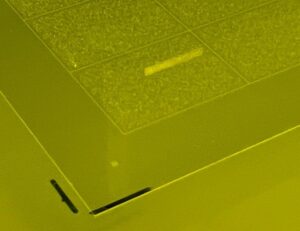
Figure 2: Glass panel with TGV.
It is also necessary to measure the thickness of the glass before starting the TGV process. Thickness uniformity across the glass panel is key. Consider this example: let us say that the thickness of a glass panel is 400µm at one end of the panel and 300µm at the other end. While this is an extreme example, you can imagine the effect that this might have on TGV height across the panel and the disastrous effect it would have on the performance of any device made from this glass substrate.
While inspecting the glass and measuring glass thickness before manufacturing begins is of considerable importance, there are a number of specific process steps throughout the TGV fabrication and metallization process where CD metrology and defect inspection are vital.
After the laser modification and etching process, manufacturers need to measure CD at the top of the via, the waist of the via, and bottom of the via;. A high-resolution, high-throughput optical panel inspection and metrology system can be used to measure these parameters for every single TGV on the panel, enabling precise monitoring of the etching process. In addition, the ability to detect defects such as incomplete etching, microcracks along individual TGV, larger cracks between multiple TGVs, and dimples and dents on the glass surface are crucial for process optimization.
In the metallization and planarization step, inspection systems can continue to monitor for defects such as residues, over/under plating, excess/insufficient polishing, and surface roughness, each of which could affect the overall electrical performance.
With millions of TGV on a panel, the ability to analyze a large quantity of inspection and metrology data within a short time period is a significant capability. The use of yield management software can shorten the time for analysis, identify systematic defects, and correlate process parameters with yield outcomes.
Conclusion
The adoption of glass core for IC substrate is currently at the starting point of what could be considerable market growth. By 2030 glass core substrate revenue is projected to grow to $275 million, according to best case scenario results from the . With the right tools on hand, manufacturers will be equipped to meet the rising demand for glass core substrates.
However, unlocking the full potential of glass core substrates and TGVs are not just about having tools; it is about using them in concert to build a process that is robust, repeatable, and yield optimized. As the adoption of glass as a substrate accelerates, manufacturers that invest in comprehensive process insight will be the ones that lead.
Monita Pau is Strategic and Product Marketing Director, Advanced Packaging, at Onto Innovation.
You Have a Challenge? Let’s talk.
We’d love to connect with you.
Looking to learn more about our innovative solutions and capabilities? Our team of experts is ready to assist you. Reach out today and let’s starts a conversation about how we can help you achieve your goals.
Let’s Talk
"*" indicates required fields
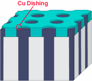
As demand grows for high-performance computing (HPC) and AI-driven applications, manufacturers are turning to hybrid bonding to enable the ultra-dense 3D integration required for next-generation chip architectures.
This advanced packaging technology presents significant process challenges. Surface preparation must be precisely controlled to eliminate particles, excess recess, and copper pad dishing, all of which can compromise bond quality. During pre-annealing, particle-induced gaps and wide bonding gaps can prevent proper wafer contact. Post-annealing, the formation of dielectric and metal voids introduces further risks to electrical performance and long-term reliability. If not carefully managed, these issues can lead to increased defectivity, reduced yield, and degraded performance in HPC and AI systems where reliability and speed are critical.
Source: AMD 3D V-Cache with TSMC SoIC 3D Packaging reverse engineering & costing report, Yole Group, 2022
Hybrid bonding reliability starts with robust process control. Monitoring topography and detecting particles, cracks, and voids help identify defects early. Measuring copper pad dishing offers insight into surface conditions and planarity. Tight control during pre-bonding steps enables potential rework before permanent defects occur.
The following examples highlight key metrology and inspection techniques that support more consistent hybrid bonding outcomes.
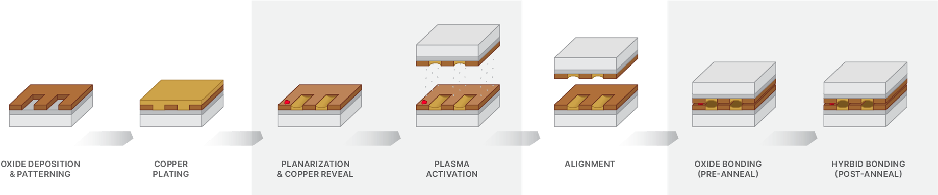
Pre-Bonding Process Control


Post-Bonding Process Control
Heterogeneous integration is a key enabler of today’s AI innovations. By bringing together multiple chips with different functionalities, a.k.a., chiplets, AI devices have been able to achieve tremendous performance gains. However, the heterogeneous integration of advanced packages has its own set of process control obstacles that must be addressed, including new interconnect challenges involving redistribution layers (RDL) and bond pads.
Recently, Onto Innovation and Samsung Electronics Co., Ltd., teamed up to explore how picosecond ultrasonic technology could be used to measure the metal thickness of RDL and bond pads in high performance AI packages. In this blog, the second in our series on the advanced packaging applications of picosecond ultrasonic technology, we will show how this technology can be used to measure metal films during RDL and bond pad processes.
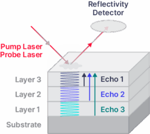
But first, a word about picosecond ultrasonic technology, a widely adopted non-contact, non-destructive acoustic technique that can be used to measure film thickness.
Measuring Films
Picosecond ultrasonic technology measures film thickness by tracking the round-trip travel time of ultrasonic waves generated and detected using an ultrafast laser pump probe technique. A short laser pulse (pump) creates an acoustic wave that travels through the film, reflects at material interfaces, and returns to the surface. A second laser pulse (probe) detects the returning wave.
Two detection methods can be used to determine film thickness or properties:
- REF mode senses changes in surface reflectivity caused by the returning wave.
- PSD mode detects surface deformation by measuring shifts in the reflected probe beam.
By measuring the time it takes for the wave to return and knowing the speed of sound in the material, the film thickness can be accurately determined to sub-angstrom levels.
This level of layer-specific metrology, precision, and measurement repeatability is increasingly critical as AI-driven packaging pushes the limits of interconnect density and uniformity.
Accuracy and Repeatability
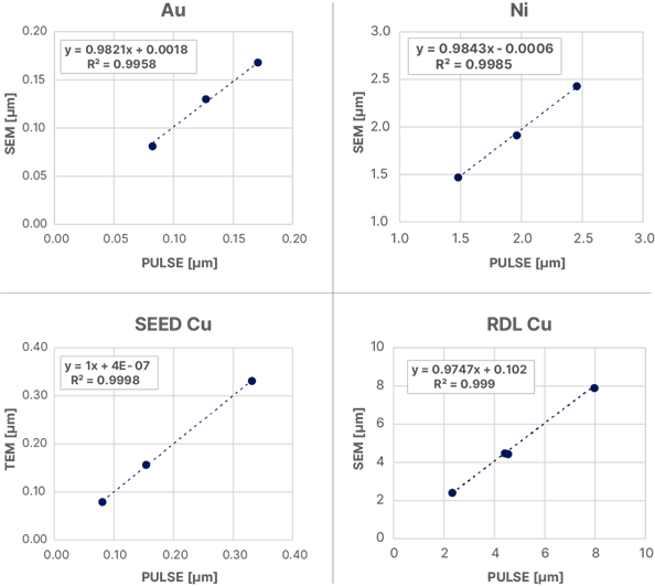
For the purpose of our exploration, we conducted a test to confirm the accuracy of picosecond ultrasonic technology when measuring the films typically used in advanced packaging. These metals include Au, Ni, physical vapor deposition (PVD) seed Cu, and RDL Cu (EP). For each film we used picosecond ultrasonic technology to measure wafers of varying thicknesses. Then we cut the wafers for cross-section analysis and estimated the correlation with the picosecond ultrasonic results for the four films (Figure 1). In this scenario, the correlation factor R2 was higher than 0.99 for all four cases, with the slope close to one, demonstrating the accuracy of picosecond ultrasonic measurements.
This level of correlation is not only impressive, it is essential. Competing technologies such as four-point probe (4PP) or contact profilometry often fall short in multilayer structures or non-planar surfaces, where mechanical contact can distort results or damage delicate features.
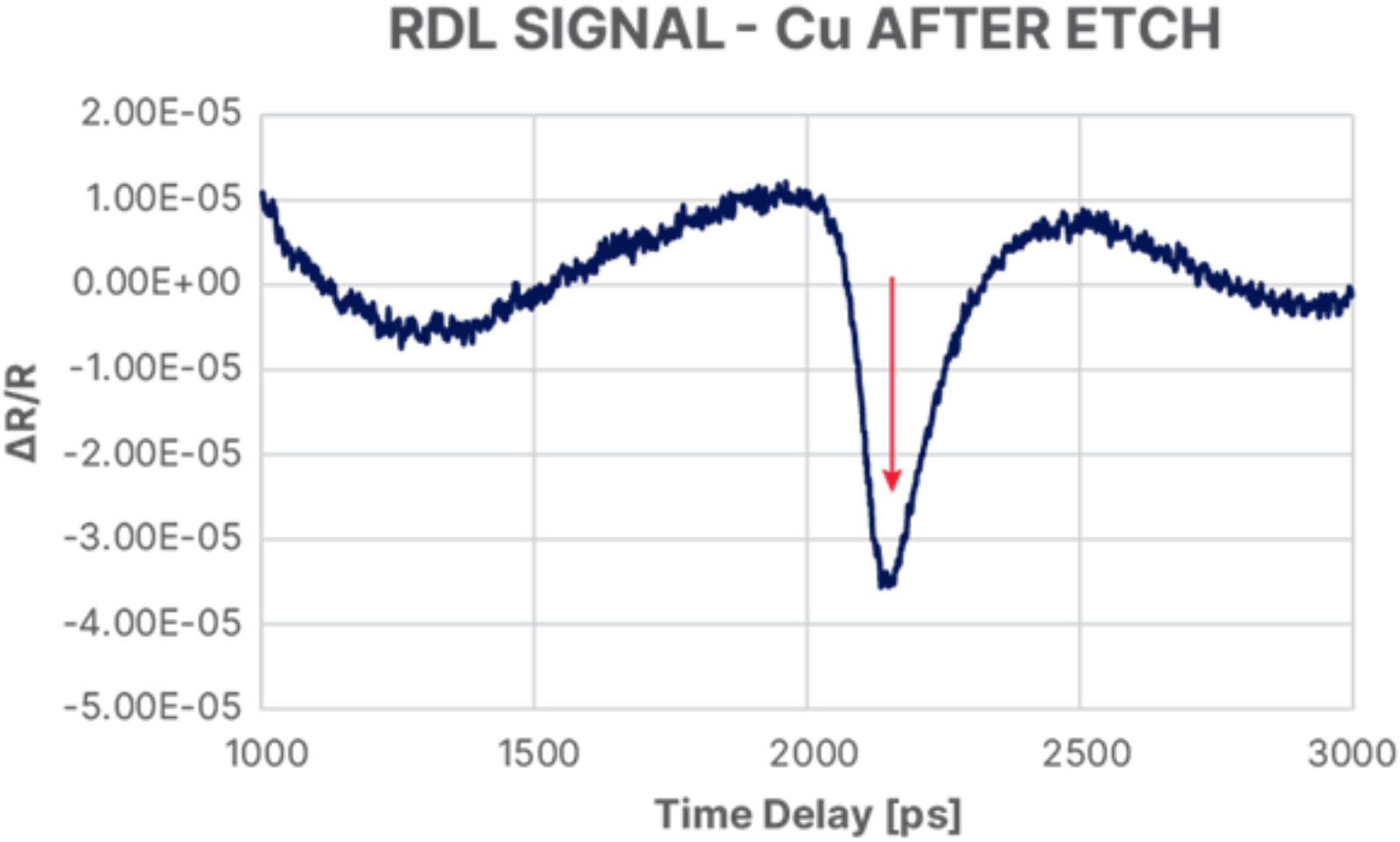
Following this, we measured product wafers in various interconnect processes with picosecond ultrasonic technology, including seed Cu/Ti measured in REF mode (Figure 2) and RDL in PSD mode (Figure 3). RDL thickness can be measured both in pre- and post-seed Cu removal.
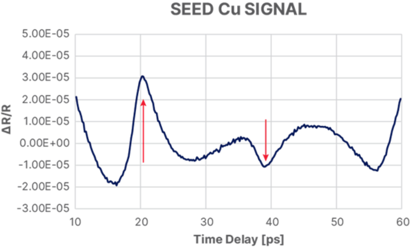
The horizontal axis in Figures 2 and 3 represents the time delay of the probe pulse with respect to the pump, while the vertical axis represents the change of reflectivity (ΔR/R) caused by the travelling acoustic wave. The sharp change of reflectivity in the signal, as demonstrated in Figures 2 and 3, is mostly due to the acoustic wave reflected from the film interface returning to the surface. In addition, the position of the peak and trough is shown with red arrows. These arrows are directly related to the thickness of the films, seed Cu, barrier Ti, and EP Cu. From the position of the peak and trough, the thickness of each film can be calculated. For seed Cu and barrier Ti, the repeatability of each layer is 0.3% or less of the thickness for all measurements. This demonstrates the capability of picosecond ultrasonic technology to meet 10% gage repeatability and reproducibility requirements.
For RDL Cu, the sharp change of reflectivity near 2,200 picoseconds (ps) corresponds to the round-trip time of the acoustic wave within the RDL Cu film; Cu thickness can be calculated from the trough position. The sharpness of the trough, along with thickness, indicates the trough position can be calculated with good repeatability. In fact, the repeatability of RDL Cu measurements for each point is less than 0.1% of Cu thickness, once again exceeding the 10% gage repeatability and reproducibility requirements.
Such precision is a necessary technical achievement. As AI applications demand tighter control over signal integrity and power efficiency, the margin for error in interconnect thickness shrinks dramatically. Legacy tools simply cannot keep up.
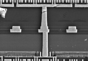
Measuring Bond Pads with Dimple Structures
We also used picosecond ultrasonic technology to measure a bond pad with a dimple structure. The film stack is composed of Au/Ni/Cu, with Au being the top film. Although the height of the center region of the pad is lower than the surrounding region by a few microns, we successfully measured individual layer thicknesses by measuring a few sites in the outer ring area and selectively choosing ones with good signal-to-noise ratios. This is possible because the focused spot size of the picosecond ultrasonic beam is 8×10µm2, small enough for the direct measurement on the outer ring of the pad.
This is another area where contact-based methods struggle. The ability to selectively target small, non-planar regions without physical interference is a key differentiator of picosecond ultrasonic technology.
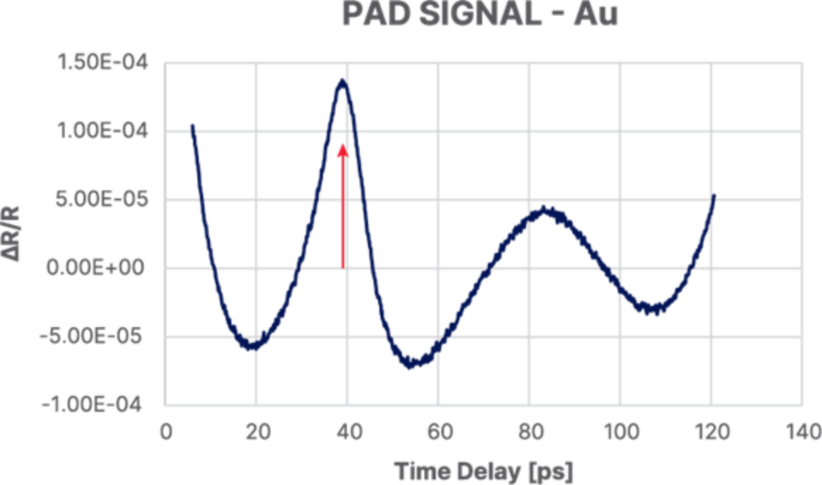
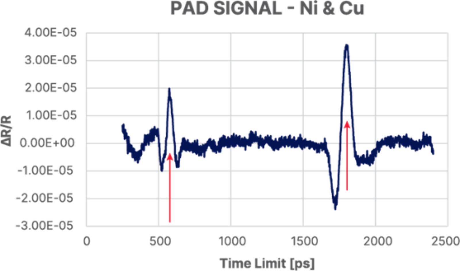
In Fig. 4 a-b, the red arrows indicate the reflectivity changes caused by the acoustic waves returning from the interface to the surface. With these peak positions, we were able to calculate each layer’s thickness with good accuracy and repeatability. The repeatability of Au, Ni and Cu films for each measurement was less than 0.2%, 0.05% and 0.05%, respectively. As such, all three film measurements outperformed the requirement of 10% gage repeatability and reproducibility.
It should be noted that Au film is much thinner than the other two films. As such, there is a significantly higher repeatability for Au films compared with the other films.
Conclusion
The AI era is upon us, and it would not be possible without advanced packaging innovations. However, the complexity of today’s advanced packaging is worlds away from traditional packaging. Today’s back-end process involves a variety of technologies and requires new methods of process control. In addition, controlling metal thickness and within wafer uniformity in these processes is critical to meeting the requirements for signal integrity in advanced packaging.
Unfortunately, some fabs still rely on legacy metrology tools like 4PP or contact profilometry—technologies that were never designed for the complexity of modern AI packages. These tools often introduce mechanical stress, lack the resolution to resolve thin or buried layers, and cannot reliably measure non-planar or dimpled structures.
As we have demonstrated, picosecond ultrasonic technology is an ideally suited interconnect metrology solution for both RDL and bond pads. This technology offers excellent accuracy and gage capability for the control of interconnect processes in advanced packaging.
As back-end processes demand the same level of precision, uniformity, and control traditionally associated with front-end requirements, picosecond ultrasonic technology can play a major role in advanced packaging metrology, delivering the non-contact, high-resolution, and repeatable measurements that AI applications demand.
Acknowledgments
We would like to thank Dae-Seo Park, Sanghyun Bae, Junghwan Kim, and Hwanpil Park of Samsung Electronics Co., Ltd., and Kwansoon Park, G. Andrew Antonelli, Robin Mair, Johnny Dai, Manjusha Mehendale and Priya Mukundhan of Onto Innovation for their contributions to this article.
About the author
Cheolkyu Kim, Ph.D., is director of product marketing at Onto Innovation with a focus on application development for picosecond ultrasonic (PULSE™) and inspection technologies. Prior to joining Onto, Kim was a postdoctoral research associate in the Physics Department of Brown University. During his three years at Brown, he spent time researching magnetically levitated superfluid liquid helium.
If you are a part of the semiconductor industry or simply someone interested in the field, you have likely heard what has become a common refrain: the back-end of the process is becoming more like the front-end of the process. In other words, the technologies that were once exclusively deployed in the first part of the process are being used to meet the increasingly stringent requirements of advanced packaging on the back of the process.
This is especially true for complex AI devices, where heterogenous integration brings together multiple chips with different functionalities. These devices present manufacturers with new interconnect challenges, especially when it concerns redistribution layers (RDL) and bond pads. This is certainly the case for high-bandwidth memory chips, some of which may feature eight to 12 interconnected DRAM chips. And those numbers are only going to climb higher, while the need to properly measure interconnects is only going to grow in importance.
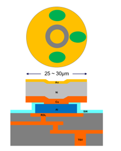
With RDL and bond pad metrology, the need to measure sites under 10μm is emerging as a new requirement. Unfortunately, traditional back-end approaches – like X-ray fluorescence or sheet resistance measurements and white light scanning interferometers – have limited capabilities that make them poor candidates for advanced interconnect process control. Measuring RDL and bond pads in AI packages requires traditional front-end metrology tools offering in-line process control capable of measuring small sites within a tight process control window (Figure 1).

The semiconductor industry has long adopted picosecond ultrasonic technology as a non-contact, non-destructive technique capable of providing accurate measurements for single-layer and multi-layer metal films. Recently, Onto Innovation and Samsung Electronics Co., Ltd., teamed up to explore how this front-end mainstay also could be used to measure metal thickness in RDL and bond pads in high performance AI packages.
In part one of this two-part blog series, we will focus on traditional techniques and current challenges, whereas in the second blog we will discuss solutions involving picosecond ultrasonic technology. But first, a quick word about the latest generation of picosecond ultrasonic technology.
Picosecond Ultrasonic Technology
In our study, we used fifth generation picosecond ultrasonic technology to measure the thickness of individual metals on multi-layer structures. To measure very rough film, pump beam intensity was modulated at 5 MHz. This modulates the intensity of the acoustic wave it generates. Then the reflected probe beam signal from the detector was demodulated with the same frequency as the pump modulation, allowing for the measurement of weak reflectivity changes caused by the acoustic wave.
As the pump beam itself does not convey any information about the travelling acoustic wave but has the same frequency as demodulation, demodulating the signal from the detector may include the signal from the pump, resulting in significant noise. This is especially the case when measuring rough films where pump beam scattering is strong. To address this, such noise can be filtered out by modulating the probe beam at a different frequency, 0.5MHz, and demodulating the signal from the detector with the sum of the two frequencies, 5.5 MHz.
Another significant improvement made to this technology is that the maximum probe beam time delay for the measurement has increased from 5 nanoseconds (ns) to 15ns. This means the maximum thickness that can be measured has increased threefold. For Cu measurement, the maximum thickness that can be measured is now 35μm.
With our discussion of picosecond ultrasonic technology out of the way, we will turn our attention to the advanced packaging needs of AI devices.
AI Packages
To create AI devices, manufacturers use heterogeneous integration to package memory and process chips together in 2.5 and 3D structures. This enables faster communication and lower power consumption.
In these structures, conventional memory chips are replaced with high bandwidth memory (HBM) and paired with a graphics processing unit (GPU). HBM enables the higher data transfer rates needed to handle the significantly increased data processing generated by parallel computation with the GPU. In the latest generation HBM, eight to 12 DRAM chips are connected to each other vertically by through silicon vias (TSV) to form one HBM package. Then four to six HBM packages are connected, horizontally, with the GPU chip by RDL on a Si interposer. These new interconnected structures offer significantly improved computing power and latency and higher bandwidth for data transfer and low power consumption. Each are needed for AI computing.
In the case of RDL on a Si interposer, manufacturing multiple layers of RDL is required to handle high data transfer rates. As such, the manufacturing process is more complex compared to the manufacturing process for mature packages.
Metals, mostly Cu, in RDL are typically deposited using the electroplating (EP) process. The thickness of the metals is affected by the geometric structure underneath, making thickness uniformity control very challenging. To meet the within wafer uniformity requirement for RDL impedance control, measuring and monitoring metal thickness directly on product wafers is crucial. As RDL lines shrink to 2µm or lower – the line/space (L/S) requirements of the most advanced packages – dimensional control is vital to device performance while process control itself becomes even more stringent.
After the final RDL layer on a Si interposer is formed, bonding pads are created. These bonding pads connect with HBM or GPU chips through micro-bumps. Like RDL, bonding pads are also created using the EP process. However, some bonding pads are flat while others possess a dimpled structure (Figure 2). To maintain process control, engineers will still need to measure metal thickness directly on both flat and dimpled structures. In the case of the latter, such measurements are a lot more challenging.
Traditional Packaging Process
During the traditional packaging process, metal film measurements are characterized using automated and semi-automated measurement tools such as X-ray fluorescence or sheet resistance measurements. While these tools are easy to use and offer low cost of ownership, they are not up to the task of measuring multi-layered films or films with varying topographies on product wafers in high volume manufacturing.
White light scanning interferometer (WLSI) systems are also used in RDL process monitoring. These methods rely on wavelength-dependent interference patterns to provide the step height of metals; this assumes that the step height is the same as metal thickness, which may or may not be true depending on the structure.
As RDL films become thinner, wavelength dependent interference patterns become less sensitive to thickness variation. This affects measurement accuracy. In the case of RDL lines 2µm L/S and lower, the accuracy of thickness measurements becomes even more critical for process monitoring and control. However, WLSI systems have shown limitations in meeting these metrology requirements.
In general, the front-end process must operate inside a window that varies within 10% of the target value. This, in turn, requires a metrology tool with a gage capability (3σ repeatability and reproducibility) of 10% of the variability or 1% of the target value. This metrology tool must be able to measure in-die areas and on test structures smaller than 50µm on real product wafers. Such a tool also needs to be non-contact, non-destructive and fast enough to support high volume production. Picosecond ultrasonic technology enables advanced packaging manufacturers to meet these challenges.
In our next blog, we will take a deep dive into how picosecond ultrasonic technology can be used to measure metal films during RDL and bond pad processes. We hope you join us as we continue to explore the advanced packaging applications of picosecond ultrasonic technology.
Acknowledgments
We would like to thank Dae-Seo Park, Sanghyun Bae, Junghwan Kim, and Hwanpil Park of Samsung Electronics Co., Ltd., and Kwansoon Park, G. Andrew Antonelli, Robin Mair, Johnny Dai, Manjusha Mehendale and Priya Mukundhan of Onto Innovation for their contributions to this article.
About the Author
Cheolkyu Kim, Ph.D., is director of product marketing at Onto Innovation with a focus on application development for picosecond ultrasonic (PULSE™) and inspection technologies. Prior to joining Onto, Kim was a postdoctoral research associate in the Physics Department of Brown University. During his three years at Brown, he spent time researching magnetically levitated superfluid liquid helium.