
When the subject of hybrid bonding is brought up in the industry, the focus is often on how this technique is used to manufacture CMOS image sensors (CIS), an essential device for today’s digital cameras, particularly those found in smartphones. As such, CIS is a common touchpoint given the ubiquity of mobile phones, whether you hold a product from Apple, Samsung or Huawei in your hands.
But while today’s CIS devices currently dominate the use of hybrid bonding, high-performance computing (HPC) is emerging as a new high-growth application for hybrid bonding. This is a result of the trend toward finer pitched interconnects in advanced 3D packaged memory technologies. In addition, the market share of high-end performance packaging, including both 2.5D and 3D packaging, is expected to be $7.87B by 2027, with a compound annual growth rate (CAGR) of 19% from 2021 to 2027, according to Yole Développement. As for 3D stacked packaging alone, it is expected to grow at a CAGR of 58% to 70% during the same period.
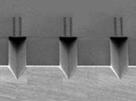
Using direct Cu-to-Cu connections instead of bumps and suitable for pitches less than 10μm, hybrid bonding often involves the direct stacking of two wafers, with the space between the two planarized surfaces approaching zero. Hybrid bonding has advantages over conventional micro-bumping, such as enabling smaller dimension I/O terminals and reducing pitch interconnects. But while both hybrid bonding and conventional micro-bumping support higher-density interconnect schemes, hybrid bonding is an expensive process compared to bumping and requires much tighter process control, especially in the areas of defect inspection, planarity measurement and void detection.
While wafer-to-wafer bonding has already been demonstrated for NAND devices and is currently used in CIS manufacturing for the integration of the imager layer and logic, DRAM manufacturers are also looking to adapt hybrid bonding to replace bumps. Utilizing a hybrid bonding interconnect scheme capable of reducing the overall package thickness by tens and possibly hundreds of microns in certain situations, HBM (high-bandwidth memory) die are vertically stacked in 4,8,12,16 die stacks. The gap between each die is about 30μm when bumps are used, but the gap is nearly zero with hybrid bonding.
Ajinomoto build-up film (ABF) substrate has been a key component in chip manufacturing since its introduction shortly before the turn of the millennium. Substrates made with Ajinomoto build-up film – an electrical insulator designed for complex circuits – are found in PCs, routers, base stations, and servers.
Looking ahead, the ABF substrate market will continue to grow, with revenue up last year due to the strong demand for 5G, high-performance computing (HPC), servers and graphic processing units (GPU), as well as from the automotive industry. According to Goldman Sachs, the total demand for the ABF market should maintain a CAGR of 28% from 2022 to 2025. Like so many other essential components in the global supply chain, there is a shortage of ABF substrates.
But rising demand and supply chain issues aren’t the only factors contributing to the shortage of ABF substrates. Larger package sizes and an increasing number of layers for these high-technology products also play a part; after all, these larger packaging sizes result in fewer packages per ABF substrate. And since the manufacturing of ABF substrate is a build-up layer process, a defect in any one layer can hamper the final yield of the entire substrate. Given these factors facing the ABF substrate market, yield control becomes even more important than it was before.
After TSMC announced plans to construct a new fab in Arizona, the Taiwan-based company disclosed that they are considering building new fabs in Japan and Germany. While the Arizona fab will focus on producing 5nm nodes using extreme ultraviolet lithography (EUV) technology, the new plant in Japan reportedly would focus on the 28nm node. This 28nm fab in Japan would be in addition to a 28nm fab expansion in China.
Given that the latter node was introduced in 2008 and is not regularly used today to build central processing units (CPU) and graphics processing units (GPU), the question arises, why is TSMC building not one, but three new fabs centered around 28nm node production? The answer is simple: customer demand.
And in this case, that demand is powered by devices and applications that use augmented reality (AR) and virtual reality (VR). Most of the devices, including those that use CMOS image sensors (CIS), are manufactured on 28nm to 80nm node technology. This is why major foundries, including TSMC and Samsung, are preparing to ramp up their volume production for these more mature nodes.
As a further illustration of the demand for the 28nm node, consider this: Apple is planning on manufacturing compact, high-resolution, micro organic light-emitting diode (OLED) display devices on silicon wafers, and Sony is planning on building image signal processing (ISP) devices; both companies will be using 28nm node technology.
AR overlays digital content and information onto images of the physical world captured by camera, and it is one of the biggest technology trends now. Apps like Snapchat and games like Pokémon GO first popularized AR, but the technology is predicted to become a part of our daily lives, influencing how we shop at brick-and-motor stores or drive (or not drive in the case of autonomous vehicles) our cars.
VR, meanwhile, is already widely used at work and home. While some gamers have embraced VR with a passion, advanced manufacturers regularly use VR to train employees. As for my company, Onto Innovation, we adopted and started using VR technology — in this case, Oculus from Facebook — for training and field support during the pandemic since some people could not meet face-to-face due to travel restrictions.
These incredible advancements in the use of AR and VR wouldn’t be possible without CIS. And with both AR and VR growing in popularity, there is no doubt that CIS applications will increase in the future.
The demand for smartphone cameras, video conferencing, surveillance and autonomous driving has fueled explosive growth of CMOS image sensor (CIS) manufacturing in the last decade. While CIS becomes an increasingly important element in the production of today’s consumer electronics, there are unique challenges in production that must be addressed. As pixel sizes shrink, we see an inverse relationship with the number of pixels in the array increasing, which presents challenges for process control of the sensor, especially as it relates to the color filter array (CFA) and on-chip lens (OCL). With the push to 1µm and below pixel sizes, the ability to find sub-micron defects and macro-level variations within the pixel array is even more important to ensure uniform and unobstructed responses throughout the active pixel sensor array (APS).
CIS is unique from other semiconductor devices because it converts light energy into electrical signals. It is manufactured on silicon wafers similar to semiconductors and follows typical back-end packaging processes such as grinding, sawing, and electrical testing. A typical CIS device has an ASP region in the center of the die with electrical I/Os (bondpads) on the periphery. Deionized water is often used to clean up mobile contamination left behind during the wafer thinning or die singulation process which has an inherent risk of staining or leaving a residue on the APS that affects the quantization of light and is considered a killer or yield limiting defect.
In their continuing drive to pack more computing power and speed into less space, semiconductor manufacturers are using advanced packaging (AP) processes to integrate multiple die of different types within a single package and to increase input/output (I/O) connectivity for large, complex chips. The use of front-end-like processes to create ever smaller features on ever larger substrates is increasing the need for process control and inspection in AP processes. Novel materials like organic polymer dielectrics pose special challenges to conventional front-end optical technologies. Our new illumination technology, Clearfind®, specifically addresses these issues to provide high-sensitivity defect detection.
Packaging evolution
Packaging processes have evolved from relatively simple, inexpensive technologies to costly, complex processes that have adopted and adapted process technologies developed for wafer fabrication. Some of these processes are discussed in the sections below.
Wire bonding. Traditionally, packaging uses thin wires bonded between I/O pads at the edge of the chip and a wire frame that includes pins for connection to a printed circuit board. The chip and frame are encapsulated for protection from the external environment, resulting in a final package that is much larger than the chip.
Flip chip. Chip-scale processes, like flip chip, form contact pads on the top surface of the die, which, when the separated die are flipped over, mate with solder balls on a connecting package substrate. Flip-chip packages allow many more I/O connections because the entire surface of the chip, not just the edges, can be used for contacts. The resulting package is smaller than wire bonding, but usually larger than the chip.
Wafer-level processing. Wafer-level processing (WLP) uses front-end-like processes to form packaging structures on chips while they are still part of the wafer on which they are fabricated. WLP has the benefit of creating small packages – the same size as the chip – but that small size ultimately limits the space available for I/O connections.
Fan-out wafer-level processing. Fan-out wafer-level processing (FOWLP) offers increased I/O capability. Separated chips are embedded in a round substrate with space added between the chips. Overlying redistribution layers (RDL) route signals from contacts on the top surface of the chip to contacts on the top surface of the larger substrate extending beyond the area of the chip itself. The round, wafer-like form factor of the reconstituted FOWLP substrates permits the use of process equipment and handlers designed for wafer processing with minimal modification. But it also limits the size of the substrate (and therefore the number of die that it can contain), and it wastes space near the curved edges of the substrate where rectangular die/packages do not fit efficiently.
Fan-out panel-level processing. Fan-out panel-level processing (FOPLP) is similar to FOWLP except the panel substrates are not limited to wafer-like form factors. They can be rectangular, to increase spatial efficiency, and larger, to process more die per panel at lower cost per die.