

Overcoming FOPLP Die Placement Error
It is well understood that advanced packaging applications require high performance, low cost, increased functionality and improved reliability that 2.5D and 3D packaging solutions provide. Fan-out panel-level packaging (FOPLP) is one of the technologies that has the potential to meet these packaging requirements. Similar to fan-out wafer-level packaging (FOWLP), FOPLP processes reconstitute die on a substrate, in this case a rectangular platform that can be significantly larger than the standard 300mm diameter wafer form. In the reconstitution process, die are displaced from their nominal grid locations during the epoxy molding compound process and sometimes during subsequent processing steps. This fan-out technology delivers more space for redistributed I/O connections, providing increased flexibility for homogeneous and heterogeneous integration. Importantly, the larger panel format can support more packages per substrate than the 300mm wafer form, and the final package size can be increased by adding space between the die.
Although FOPLP processing has many advantages, it also faces significant challenges. One critical challenge is die placement error, which occurs when die are positioned during the reconstitution and molding process. These placement errors are amplified with the larger panel format when compared to reconstituted wafers, and errors of 50μm or more are not unusual. In order to guarantee acceptable yield, these errors must be corrected during the lithography process using site-by-site corrections. Conducting metrology and site-by-site exposures on the lithography system is very time consuming. Substrate alignment and error correction may be calculated using global alignment, but this correction does not accommodate nonlinear die placement errors. It has become clear that only site-by-site corrections can deliver the overlay required to maintain good yield. Executing site-by-site alignments in the stepper reduces throughput and increases cost enough to make that approach to FOPLP processes impractical. A new approach uses an external metrology tool to capture die placement error data from a panel and feeds that information forward. The “feed-forward” solution optimizes the stepper, site-by-site, for X, Y and rotation offsets, during exposure. Visualization of the metrology data allows the user to characterize upstream and downstream processes. Moreover, analytical capabilities predict yield as a function of exposure field size, thereby allowing the user to balance throughput against yield in real time. This solution can significantly increase stepper throughput, reduce cost and increase productivity while ensuring high yield.
Die placement challenges
Generating reconstituted panel substrates creates translational and rotational die placement errors. The “pick and place” process itself introduces initial errors that are exacerbated during the mold process, and by instability of the mold compound throughout repeated processing cycles. With redistribution layer (RDL) features currently achieving dimensions as small as 2μm, die placement measurements and pattern overlay registration requirements are continuing to tighten. As a result, the position of the die must be measured before each exposure in the lithography system to ensure accurate registration with the underlying layer. Displacement errors can be measured in the lithography tool, but these measurements are slow, typically taking as much time as the exposure itself. Transferring the measurement operation to a parallel, independent metrology system and feeding corrections to the stepper, however, can double throughput. Figure 1 illustrates the use of this exposure/measurement loop to increase productivity. The die placement measurements and analysis can be repeated, if required, after each layer is exposed, to correct for any errors introduced in that step. In addition to feed-forward corrections, the software algorithm analyzes the displacement errors to predict yield (based on a user designated limit for acceptable registration error) for exposure fields of varying sizes. The method requires tight integration of the stepper and measurement system with the controlling software algorithm.
Coordinate systems; measurement accuracy
A previous study [1] looked at wafer substrates and focused on proving that automated optical inspection (AOI) feed-forward data could correct for the predefined die placement offsets. It established the AOI feed-forward accuracy to be within +/-2μm. The work described below uses a 510mm x 515mm x 1.1mm rectangular glass panel as the test vehicle to match the stepper and AOI panel stage grids and measure the AOI accuracy. The test panel was patterned using the same method as the wafer study. The test reticle used a single die “Pad” image, which was patterned across the entire panel. The pad test pattern (Figure 2), with no offsets, was then measured using the stepper and AOI system at two points per die (top and bottom).
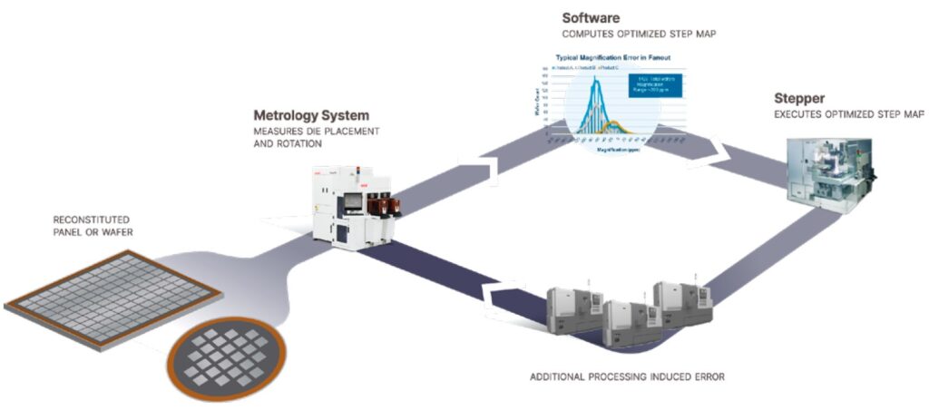
Figure 1: The optimized stepping process loop includes: 1) measurement of die displacement errors outside the stepper; 2) Site correction calculations/yield modeling; and 3) exposure.
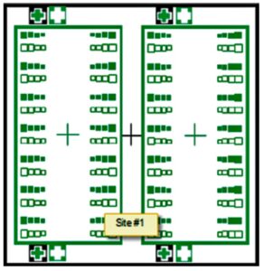
Figure 2: Pad test pattern showing two die.
The lithography system (JetStep System, Onto Innovation) supports panel sizes up to 720mm x 600mm. It uses pattern recognition alignment, allowing the user to train the system to recognize and align on any unique pattern within the field of view. The alignment system can measure the X, Y position of die patterns across the panel, a process often referred to as “mapping.” The AOI system (Firefly System, Onto Innovation) uses a similar pattern recognition alignment method to assess die placement error. Using the stepper and AOI alignment site measurements from the test vehicle panel, a mathematical algorithm was applied to align the stepper and AOI coordinate systems. Once a common grid coordinate system was established, the stepper stage was considered as the reference and the AOI system was compared to this reference using simple scatter plots (Figure 3). The measurements were repeated three times to confirm repeatability. In all three cases, accuracy of the AOI system was within +/-2.3μm of the stepper reference. Figure 4 shows histograms of the dX and dY distributions for R1. Table 1 summarizes the statistical data for each run.
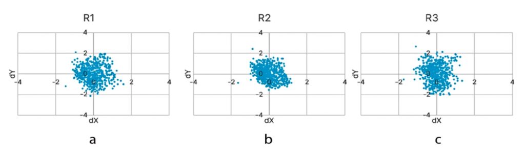
Figure 3: Scatter plots stepper vs. AOI, for three runs: a) R1, b) R2, c) R3.
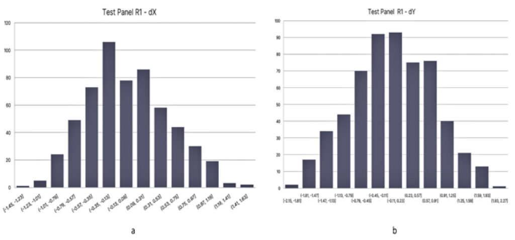
Figure 4: Test vehicle AOI error distributions R1 for a) dX, and b) dY.
Die placement error measurement
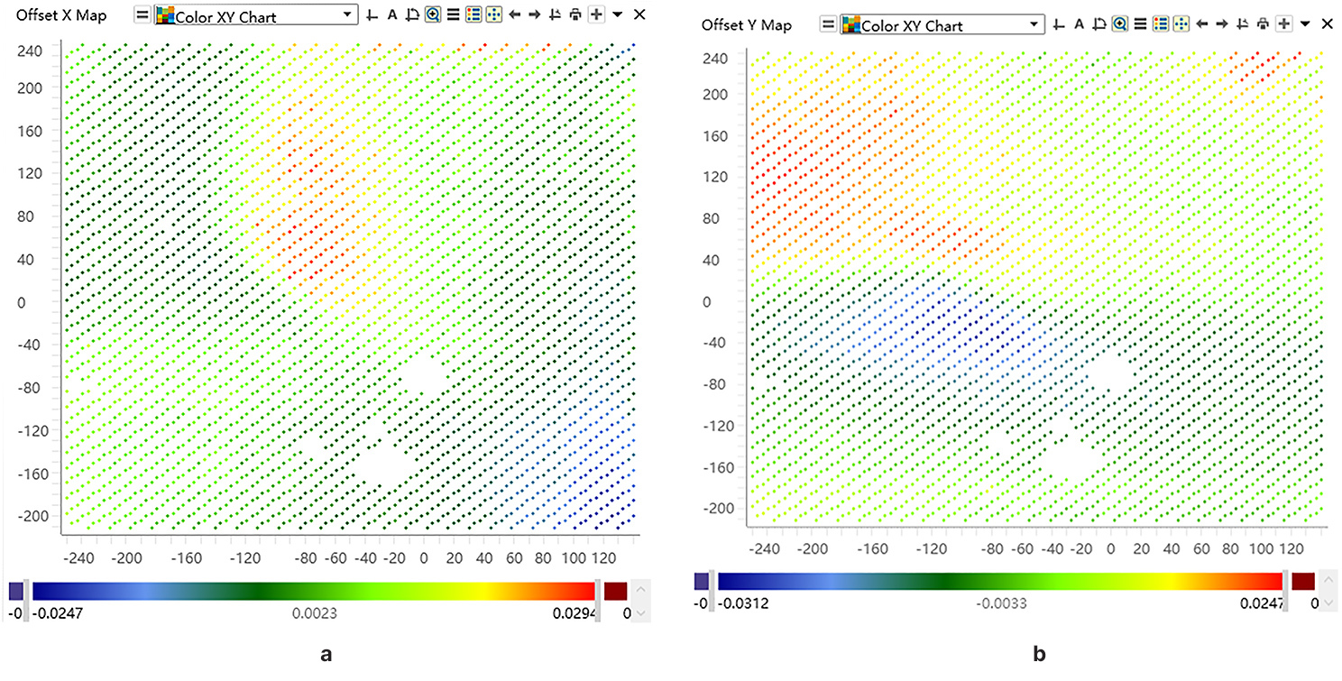
With the accuracy of the measurements and the correspondence between the exposure and measurement coordinate systems established, it is possible to evaluate the placement errors of die on FOPLP panels. Dummy die embedded in molding compound to form a FOPLP substrate were supplied courtesy of ESWIN. Measurements of two points for every die, top and bottom, allowed the system to calculate translation (X,Y) and rotation (ϴ) offsets for each. The software algorithm generates “heat maps” that visualize the dummy measurements before corrections are applied (Figure 5). Histograms of the X and Y placement errors and rotational errors (Figure 6) show the distributions of these measurements. The multimodal distributions of the dX and dY histograms reflect the nonlinear die placement errors observed in the heat maps. This nonlinear error can be attributed to the epoxy molding compound (EMC) curing process, which is typical for most FOPLP reconstituted panel processing. The disruptive EMC curing effect renders the typical global alignment solution used by lithography tools useless, as it assumes linear corrections for scaling, rotation, or orthogonality. Only site-by-site corrections can accommodate these types of errors. To apply site-by-site corrections, each exposure needs to be matched to the local errors to provide good overlay.
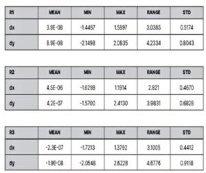
Table 1: Summary of dX, dY error statistics for R1,
R2, R3.
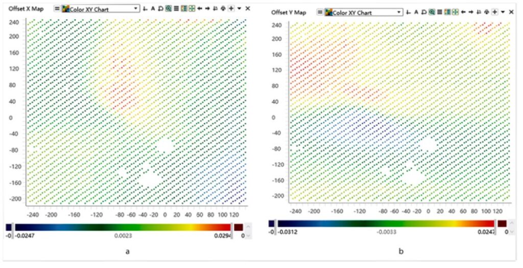
Figure 5: Die placement error (mm) a) dX, and b) dY heat maps.
Data analysis, yield prediction and throughput
The process specifies overlay errors less than +/-15μm. As long as the measured errors are within the correction capability of the stepper, it is possible to yield 100% by correcting each die, so-called “die-by-die” exposure individually, but this imposes an unacceptable penalty on stepper throughput. Increasing the size of the exposure to cover multiple die will Increase throughput, but reduces the ability to correct for individual die placement errors. By evaluating virtual exposures for different field sizes – and with each exposure corrected to optimize yield within the exposed field – it is possible to maximize process yield (defined as the percentage of die that will meet the overlay specification) and quantitatively evaluate trade-offs between yield and throughput for different field sizes. Only by having real-time data analysis can the user identify the correct settings and react to out-of-control situations without impacting yield.
For the panels evaluated, the software algorithm predicted 100% yield with a field size of 3×3 (Figure 7). The dX data was worse than the dY data, but all die placements were within the +/-15μm via to pad overlay specification. As the stepper field size was increased to 6×6 die, the yield drops to 99.42% as some of the die dX overlay errors exceeded the +/-15μm specification (Figure 8).
The software algorithm’s yield prediction has been compared to actual customer product overlay measurements, confirming the accuracy of the prediction is within 0.2% of final overlay results. This result provided the user with confidence that AOI pre-measurement of panels with product die can be used to determine the optimum field size, throughput and yield prior to coating the panel with polyimide or photoresist. This has significant advantages in both cost and process development. For example, polyimide processing is normally a non-reworkable process step and overlay errors at this stage result in scrapped die. Typically, if there is a die placement error that exceeds the specification of the multi-die exposure field it will only be observed after fully processing the polyimide lithography and measuring overlay. By this time, it would be too late to recover, requiring the die to be scrapped. With the ability to pre-measure and predict the yield with the AOI system and software algorithm, low yield could be avoided by reducing the field size. Moreover, the heat map and histogram data could be sent “upstream” to the EMC process engineer to address the root cause of molding process die placement error excursion.
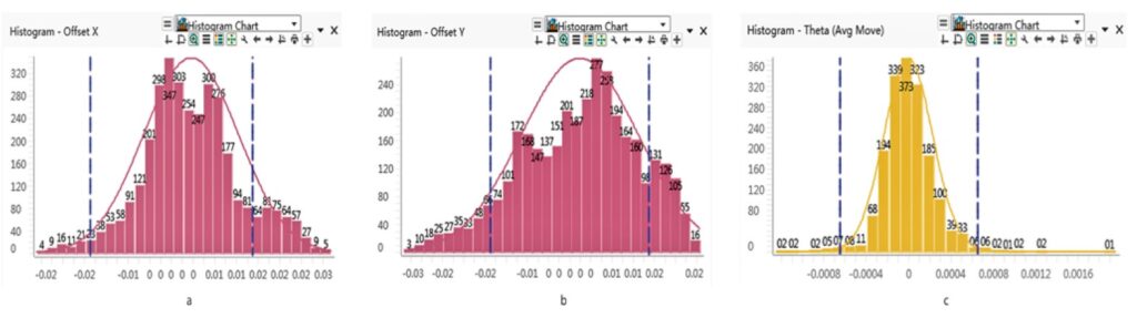
Figure 6: a) dX (mm), b) dY (mm), and c) rotation (rad) data histograms.
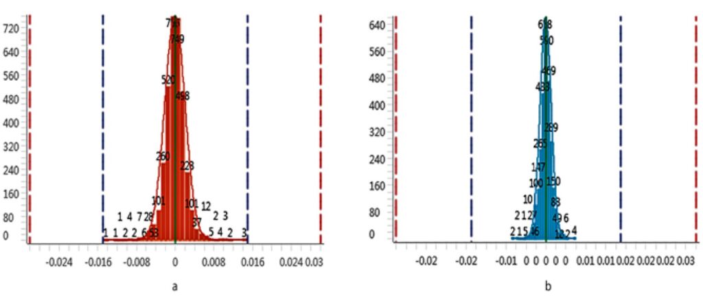
Figure 7: Predicted a) dX and b) dY overlay data histogram (mm) for 3 X 3 field, 100% yield.
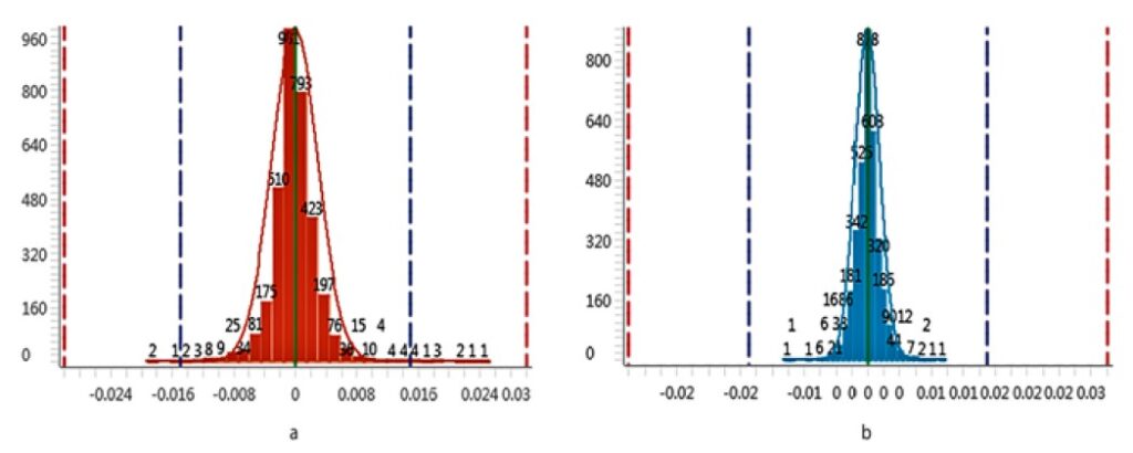
Figure 8: Predicted a) dX and b) dY overlay data histogram (mm) for 6×6 field size, where some die are out of
specification, thereby reducing yield.
Summary
It is clear from the experimental data that the calculated feed-forward site corrections provided the stepper with the ability to automatically compensate for die placement error. This is a significant improvement over the industry standard, where steppers use a simple linear model approach. Application of the site corrections, with larger field sizes during stepping, increased the lithography throughput significantly from 3 x 3 to 6 x 6 with low impact on yield, 100% to 99.42% respectively. This will naturally deliver commensurate reductions in cost of ownership. The visualization of the die placement data using heat maps, histograms, vector plots, etc., provides the process engineer with the ability to optimize and predict the impact of stepper field size on production yield and throughput. Moreover, this revolutionary capability provides foresight, enabling the user to quickly feed data to upstream and downstream processes to prevent costly rework and scrapped product. Future software developments will provide a method to dynamically balance throughput with yield.
Acknowledgements
This article is based on a paper presented at the International Wafer Level Packaging Conference (IWLPC) 2019. The authors wish to thank Amr Hafez, Phil Convey and Karie Li for their work on the software algorithm, which was key to delivering the die placement error solution, Burhan Ali for his support of the AOI system, and Corey Shay for his stepper support. Finally, we thank ESWIN, which provided the dummy die panels necessary for the yield prediction tests.
References
1. K. Best, M. Marshall, “Advanced packaging metrology and lithography that overcomes FOWLP/FOPLP die placement error,” IWLPC 2018.
2. K. Ruhmer, “Lithography challenges for 2.5D interposer manufacturing,” ECTC 2014, Orlando, FL, USA.
3. R. McCleary, “Panel-level advanced packaging,” ECTC 2015, Las Vegas, NV.
4. K. Ruhmer, P. Cochet, R. McCleary, “Panel-based fan-out packaging to reduce Costs,” SMTA/Chip Scale Review, IWLPC, San Jose, CA, Nov. 11-13, 2014.
5. K. Ruhmer, P. Cochet, R. McCleary, N. Chen, “High-resolution patterning technology to enable panel-based advanced packaging,” IMAPS 2014, San Diego, CA, Oct. 13-16, 2014.
Biography
Keith Best is Director of Applications Engineering for the lithography business unit at Onto Innovation, Wilmington, MA. He has over 30 years of semiconductor processing experience and has held a variety of Applications positions for both device manufacturing and capital equipment companies. Keith received his BSc Honors degree in Materials Science from the U. of Greenwich, UK. He holds 16 US patents in the areas of photolithography and process integration. Email [email protected]