Firefly® G3 System

The Firefly G3 system provides automated inspection and 3D metrology for advanced IC substrates and panel level packaging, delivering high resolution and productivity for demanding applications like high-performance computing (HPC), artificial intelligence (AI), cloud computing and machine/deep learning.

Firefly® G3 System

Product Overview

The Firefly G3 platform offers multiple imaging modes, including Onto Innovation’s patented Clearfind® Technology, a technique to detect residue defects on metal and metal defects on organic layers. The combination of high sensitivity inspection, 2D/3D metrology and on tool color image capture capability in a single platform reduces capital investment requirements and provides a reliable pathway for panel-based process applications that require high I/O counts and multiple-chip integration.

Integration with Onto Innovation’s Discover® Defect and TrueADC® software quickly turns defect data into actionable process control, improves defect classification and reduces manual review. It enables our customers to develop, learn and analyze new processes reliably while significantly improving their product delivery time to market.

Applications

  • Advanced IC Substrates (AICS): CCL and Glass
  • Fan-out Panel Level Packaging (FOPLP)
  • Interposers
  • Embedded Die substrates/ Interposer
  • 2.5D/3D integration
Related Products
View all
discoverdefect_feat

Discover® Defect Software

Integrated defect management system that works seamlessly with Onto tools and your entire enterprise, bringing data together for greater visibility and cleaner operation.
View Product
discoverreview_feat

Discover® Review Software

Your smart factory’s human classification interface.
View Product
stepfast_feat

StepFAST® Software

An advanced feed-forward lithography software solution for fan-out panel level packaging that enhances yield and throughput by correcting die placement errors through external measurements, predictive analytics and adaptive shot control.
View Product
Related Insights & Resources
View all
intellignet innovation oct 2025 fig 4

Through the Glass: Why the Rapid Development of TGV Demands Rigorous Analysis

Learn more
roadmap

The Innovations Driving the Advanced Packaging Roadmap, Part 1

Learn more
Default product image

Onto Innovation’s PACE Partners Talk About Collaborating on Panel-Level Packaging

Learn more
20240930_Onto_00461

Picking up the Pace of Panel-level Advanced Packaging at Onto Innovation

Learn more
the-long-climb

The Long Climb: Bringing Through Glass Vias (TGV) to High-Volume Manufacturing

Learn more
chip-scale-review

Using 2D/3D Technology to Overcome Challenges of Large-Area Panel Inspection and Metrology

Learn more
Picture1_240318_155910

How AI is Helping Optimize AI Chip Production

Learn more
chip-sacle-review

Optimizing Advanced IC Substrates (AICS) for PLP

Learn more
glass-substrate

The Glass Substrate Question: When Will It Replace Copper Clad Laminate?

Learn more
overlay

Addressing Copper Clad Laminate Processing Distortion Using Overlay Corrections

Learn more
illumina

Illumination Inspection Technology for Defect Detection on Advanced IC Substrates

Learn more
Address-image

Addressing Total Overlay Drift In Advanced IC Substrate (AICS) Packaging

Learn more
Default product image

Nip the Defect in the Bud: Using an external inspection system and FDC software increases ABF substrate yield

Learn more
fig-5_220126_110608

Outlier Control Technology and Feedforward Lithography Can Boost FOPLP Yield

Learn more
Picture1_210722_090506

Advanced Outlier Die Control Technology in Fan-Out Panel Level Packaging Using Feedforward Lithography

Learn more
defects-on-600mm

Revealing Invisible Defects on Large 600mm Panels

Learn more
overlay-results

Adaptive Shot Technology To Address Severe Lithography Challenges For Advanced FOPLP

Learn more

Do you have a Firefly G3 system question? Let’s talk!

As your partner for innovative solutions, we’re always here for you.

Discover how our cutting-edge semiconductor solutions are engineered to meet your most complex challenges: delivering performance, reliability and innovation where it matters most.

Let’s Talk

"*" indicates required fields

This field is for validation purposes and should be left unchanged.

Dragonfly® G3 System

The Dragonfly G3 system is resetting the industry’s expectations for throughput, accuracy and reliability. Combining 2D and 3D technologies, the system detects yield-robbing defects and measures features critical for today’s semiconductor technologies

Dragonfly® G3 System

Product Overview

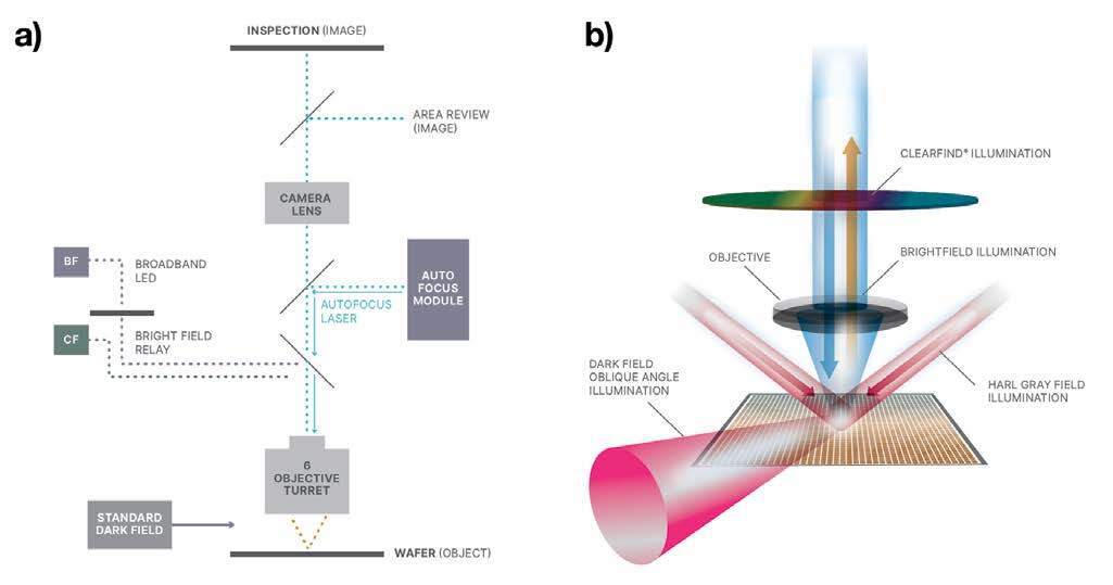
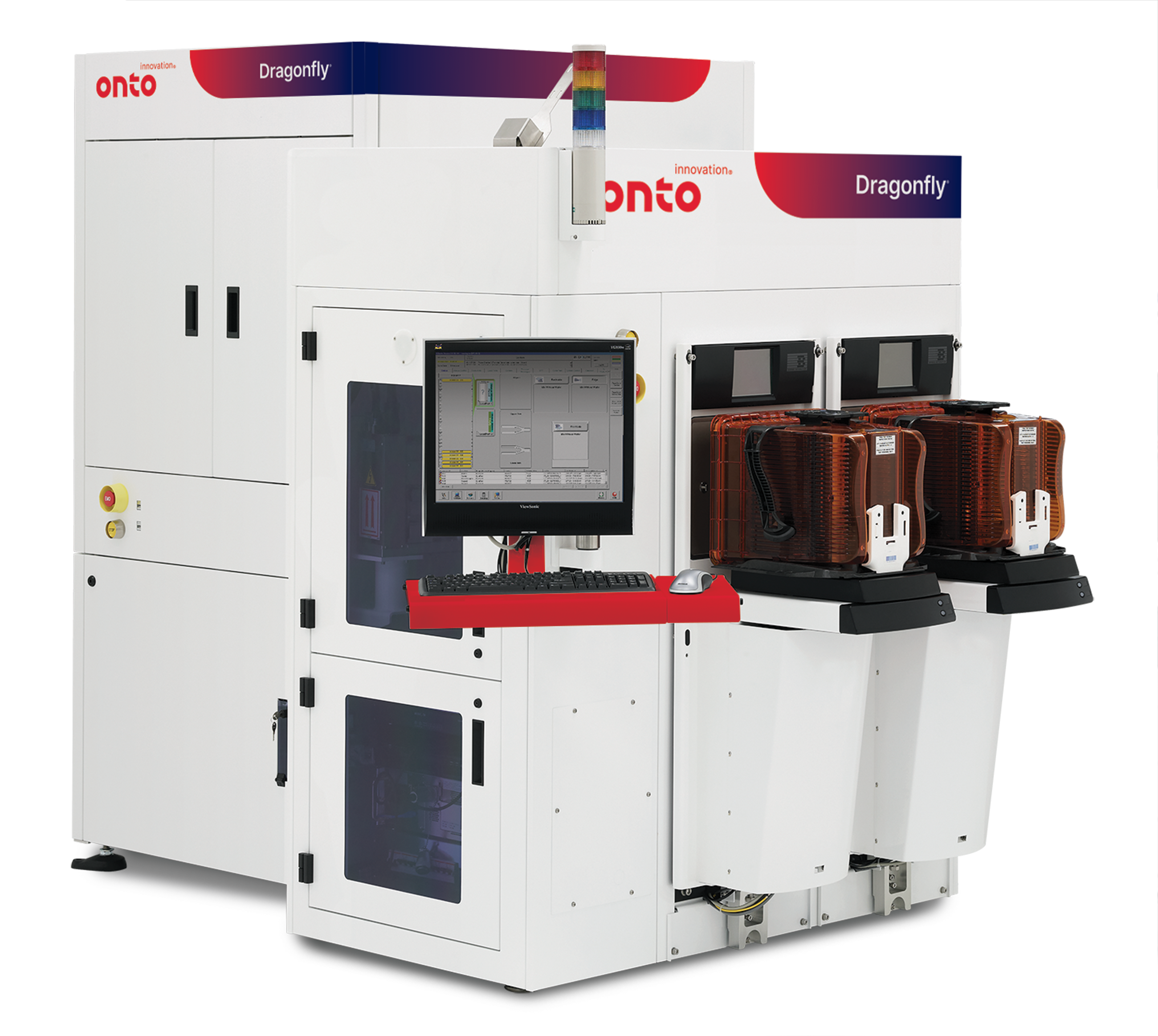
The Dragonfly G3 is a widely adopted pattern inspection system that utilizes line scan imaging technology to deliver fast, sub-micron defect detection for both R&D and high volume manufacturing environments. It features multiple illumination channels, including brightfield, darkfield, high-speed IR for embedded defects, and Clearfind® technology for detecting non-visual organic residues. Powered by modern machine learning algorithms, the Dragonfly G3 system offers a complete on-tool solution for defect detection, nuisance reduction and classification.

The system offers additional flexibility through the integration of multiple 3D metrology capabilities, including film thickness and structural profiling, and substrate thickness measurement. It features the latest 3Di technology, delivering and precise bump height metrology. The Dragonfly G3 system, with optional edge and backside inspection via the EB40 module, offers a comprehensive all-surface inspection solution for both front-end and back-end OQA.

Applications

  • Redistribution layers (RDL): after develop, after etch
  • Reconstructed and bonded wafers
  • Micro bumps and Cu pillars
  • Post saw
  • Gel and waffle pack inspection
  • Post probe and testing
  • OQA
Related Products
View all
dragonflyg5_feat

Dragonfly® G5 System

The latest generation inline pattern inspection system in the Dragonfly series, delivering sub-micron defect detection and high resolution 3D metrology.
View Product
discoverdefect_feat

Discover® Defect Software

Integrated defect management system that works seamlessly with Onto tools and your entire enterprise, bringing data together for greater visibility and cleaner operation.
View Product
discoverreview_feat

Discover® Review Software

Your smart factory’s human classification interface.
View Product
trueadc_feat

TrueADC® Software

Automated defect classification software with deep learning, real defect modeling and seamless integration with Onto AOI tools.
View Product
inspectiontoolproductivitysoftware_feat

Inspection Tool Productivity Software

Software solutions to increase the value of your inspection tool.
View Product
Related Insights & Resources
View all
Default product image

Enabling In-Line Process Control for Hybrid Bonding Applications

Learn more
Pocast-3D-InCites

Addressing The Challenges of Metrology for Advanced Packaging

Learn more
Picture1_240318_155910

How AI is Helping Optimize AI Chip Production

Learn more
Default product image

The Age of Hybrid Bonding: Where We Are and Where We’re Going

Learn more
Default product image

Center Stage: The time for hybrid bonding has arrived

Learn more
ABF-under-film-particle

Addressing The ABF Substrate Shortage With In-Line Monitoring

Learn more
watermark

In The Spotlight: What Is Responsible For The Surging Demand For CIS?

Learn more
Onto_CIS-optical-inspection-fig2

Understanding Optical Inspection For CIS

Learn more

Do you have a Dragonfly G3 system question? Let’s talk!

As your partner for innovative solutions, we’re always here for you.

Discover how our cutting-edge semiconductor solutions are engineered to meet your most complex challenges: delivering performance, reliability and innovation where it matters most.

Let’s Talk

"*" indicates required fields

This field is for validation purposes and should be left unchanged.

NovusEdge® G2 System

The NovusEdge G2 System offers fast, reliable edge, notch and backside inspection for 300mm unpatterned wafers, utilizing modular configurations.

NovusEdge® G2 System

Product Overview

The NovusEdge G2 System provides high sensitivity inspection for the edge and backside of unpatterned wafers for current and advanced nodes. Configurable modules on the same automation platform increase throughput while maintaining a small footprint for improved cost of ownership. The edge-gripping handling solution for both automation platform and the inspection modules provide desired cleanliness required for manufacturing. Optional high-sensitivity notch inspection can be added. Defects are automatically classified and binned at run time to reduce manual review.

Designed as a multipurpose inspection and sorting system for end of line outgoing quality inspection of 300mm unpatterned wafers, the system identifies, inspects and sorts wafers according to recipes.

The NovusEdge G2 system offers higher sensitivity than the previous generation, with sub-micron resolution and increased throughput by over 15%. User interaction is simplified, and the new electrical design consumes less power.

Applications

  • In-process unpatterned wafer sorting (grading)
  • Incoming wafer inspection
  • Tool qualification and monitoring
Related Insights & Resources
View all
mystery

A Bare Wafer Mystery: Inspecting for Back, Edge and Notch Defects in Advanced Nodes

Learn more
Hunting-Image

Hunting For Macro Defects: The Importance Of Bare Wafer Inspection

Learn more

Do you have a NovusEdge G2 system question? Let’s talk!

As your partner for innovative solutions, we’re always here for you.

Discover how our cutting-edge semiconductor solutions are engineered to meet your most complex challenges: delivering performance, reliability and innovation where it matters most.

Let’s Talk

"*" indicates required fields

This field is for validation purposes and should be left unchanged.