
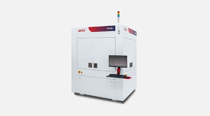
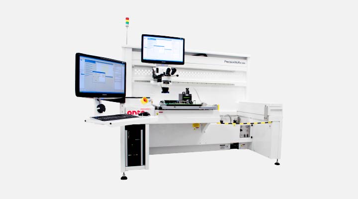
Dragonfly® G3 System
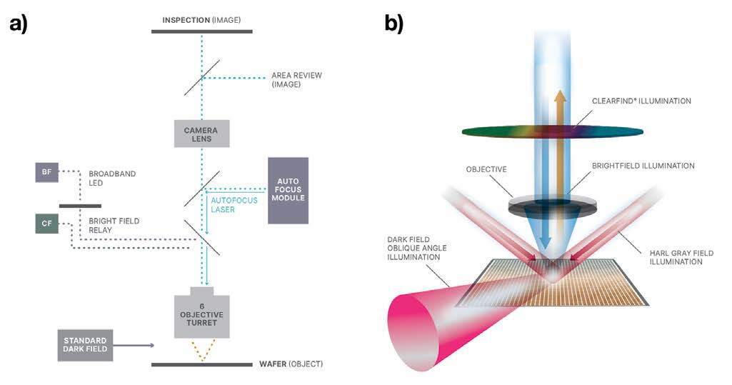
Highly configurable, automated, high speed 2D inspection and 3D metrology for inline process control in advanced packaging, specialty and front-end OQA.

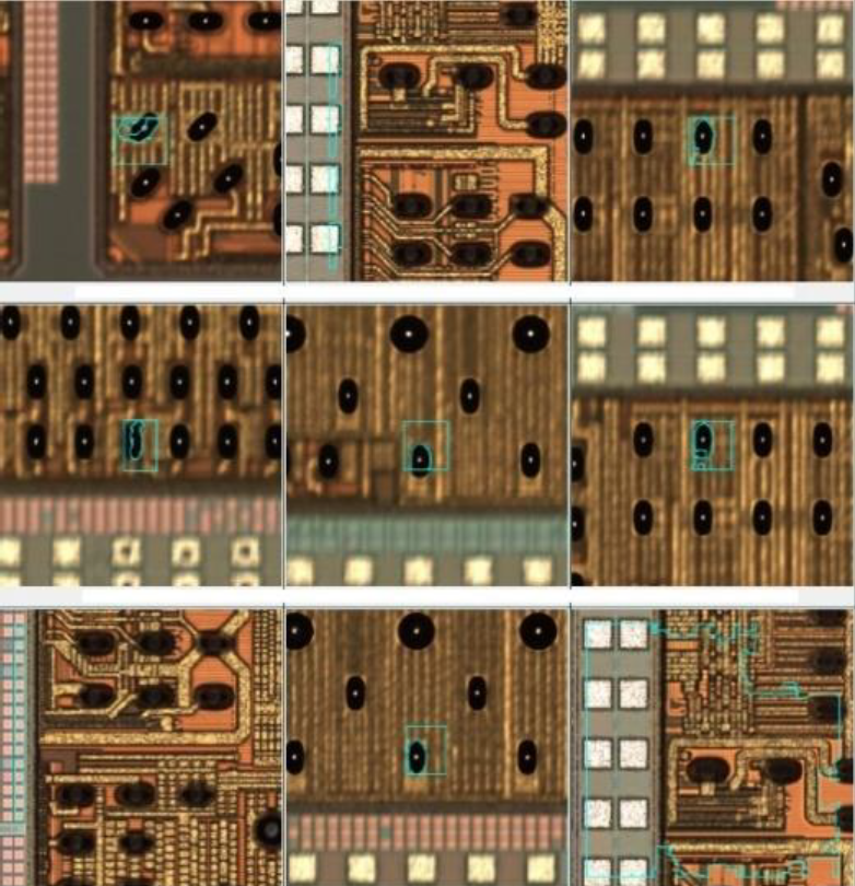
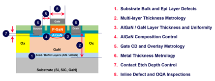
Specialty devices are the unsung heroes of modern life. For many in the semiconductor industry today, the spotlight is on the SiC and GaN power devices used in automotive, green energy, fast-charge consumer electronics (CE), and high-performance computing (HPC) applications.

May 5 — May 7, 2026
Onto Innovation is a proud exhibitor at SEMICON Southeast Asia.
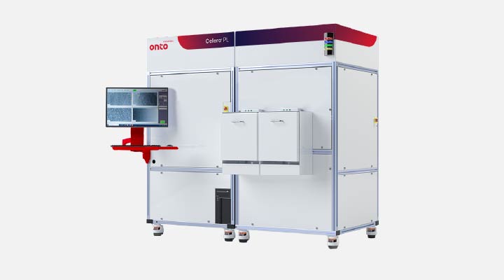
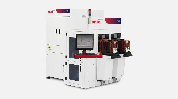
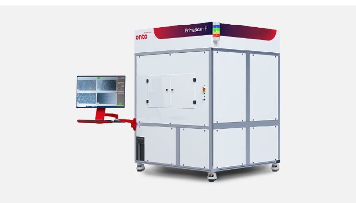
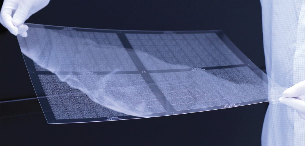
Automated, high-speed defect inspection and actionable data analysis for unpatterned wafer, patterned wafer and panels.
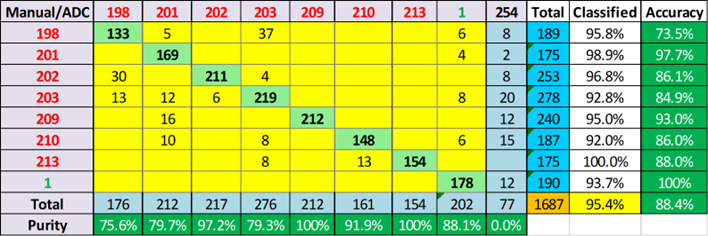
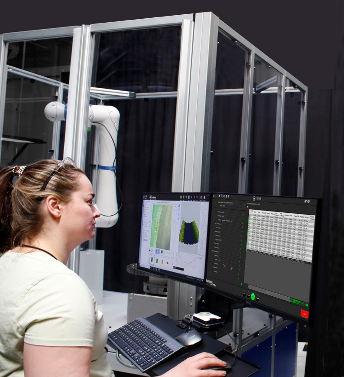
Microelectronics manufacturers partner with Onto Innovation to develop solutions to their most difficult process control challenges. We help improve yield and reliability through high-speed, automated inspection and process control software that transforms defect data into actionable insights.
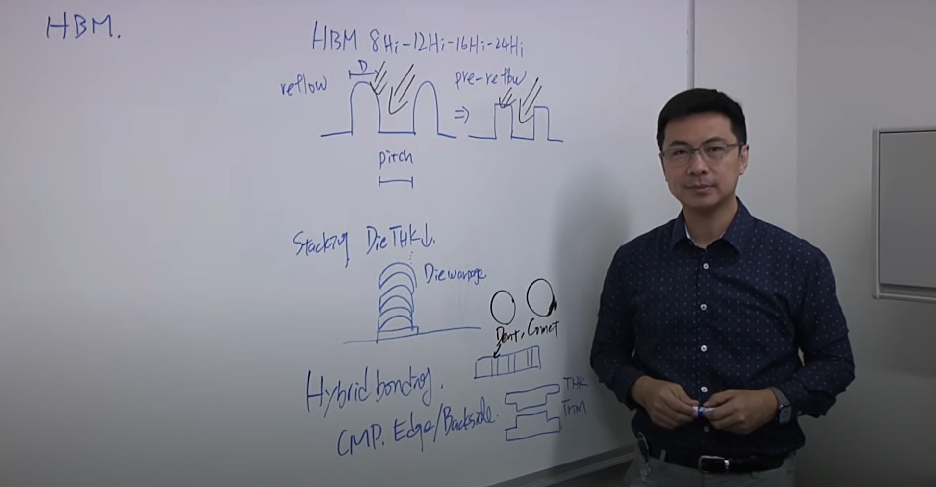
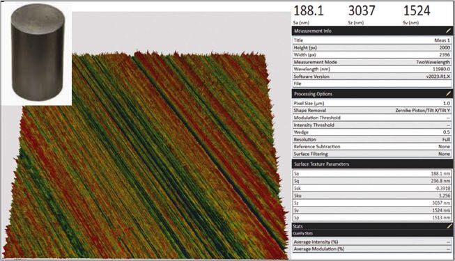
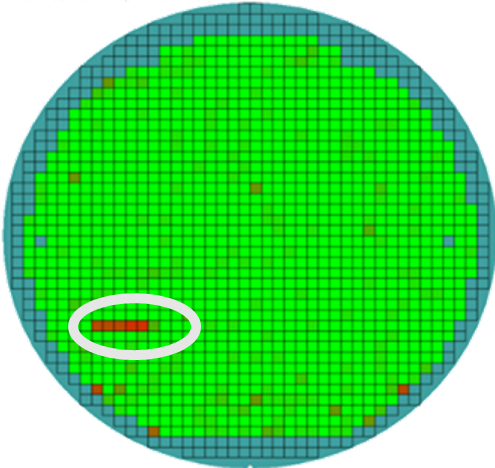
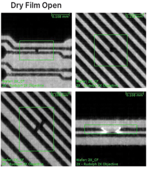
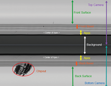
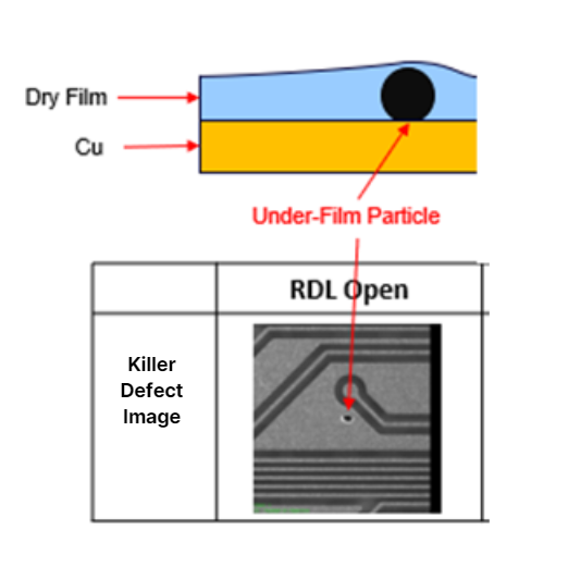
Wafer manufacturers rely on our unpatterned defect inspection solutions to ensure wafer quality, covering frontside, bevel/edge, notch and backside inspection. Likewise, chip makers need tools for macro defect inspection of patterned wafers, panels and stacked die packages to help ensure high yielding processes and an optimized cost of ownership.
From R&D to high volume manufacturing, we’re committed to helping customers realize their full potential.


As your partner for innovative solutions, we’re always here for you.
Discover how our cutting-edge semiconductor solutions are engineered to meet your most complex challenges: delivering performance, reliability and innovation where it matters most.
"*" indicates required fields