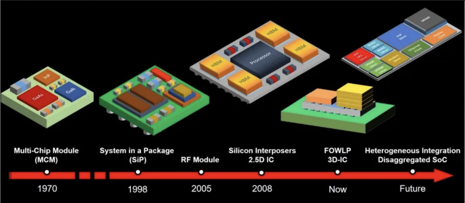
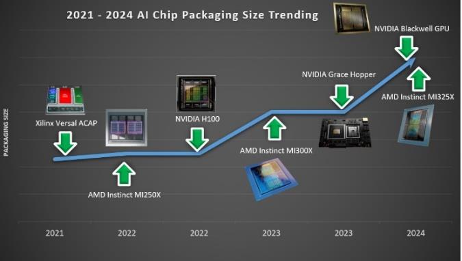
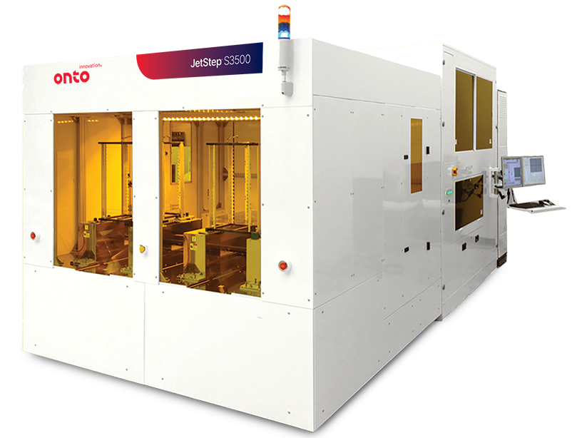
If you’ve been following the evolution of advanced packaging, you know that the industry is pushing boundaries like never before. From high-performance computing to industry-upending AI devices, the demand for smaller, faster, and more powerful chips is driving innovation at every level. One of the unsung heroes in this transformation: Glass carriers.

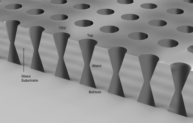
These carriers are becoming essential for applications involving high-bandwidth memory (HBM), 2.5D/3D integration, and chiplet architectures. During the manufacturing process, glass carriers serve as mechanical support for thin wafers and panel-level packages. Why? Glass carriers are noted for their warpage resistance, superior rigidity, and thermal stability. This combination of glass’ exceptional flatness and rigidity enables the precise placement of dies and interposers. Additionally, glass is optically transparent, which allows through-glass alignment during bonding and stacking, a critical capability for 3D integration where multiple layers must be accurately registered.

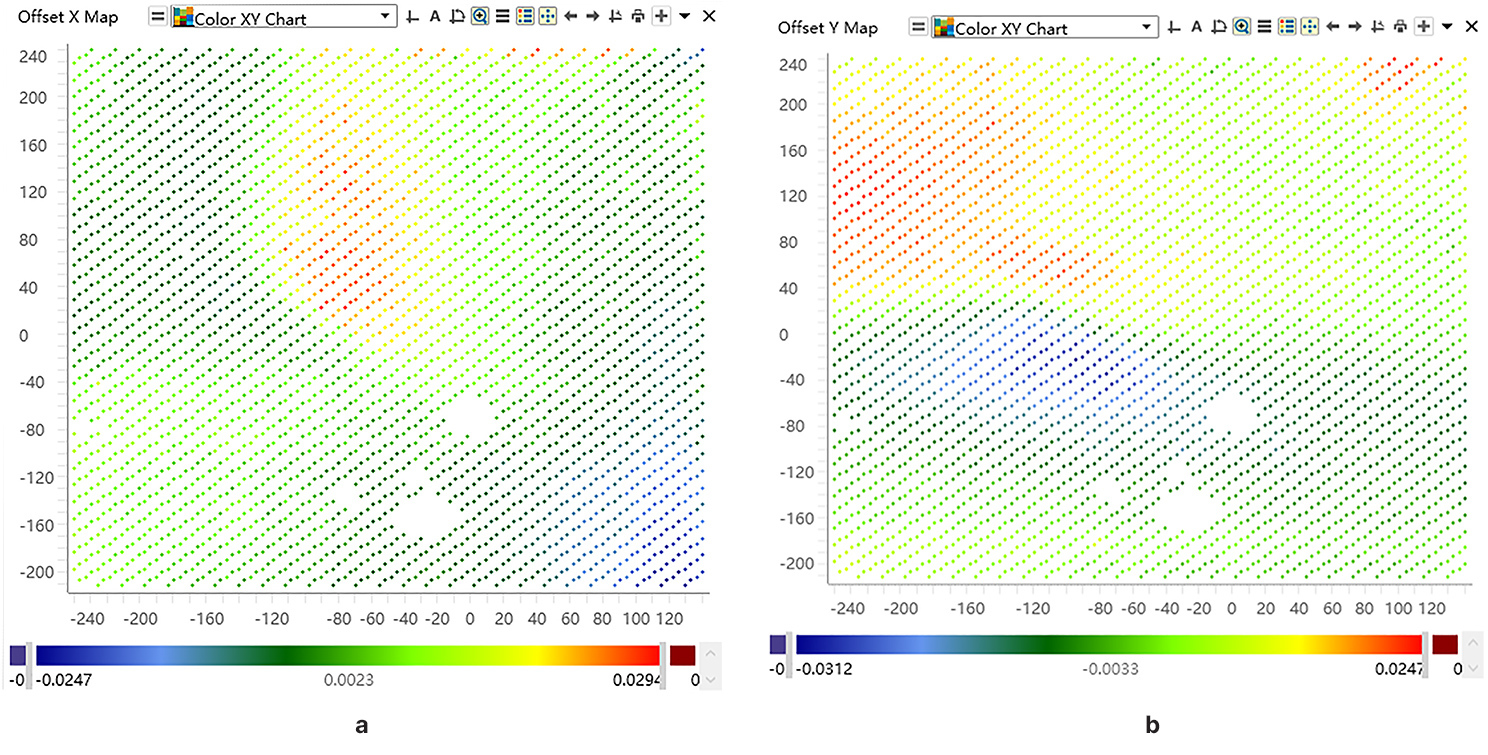
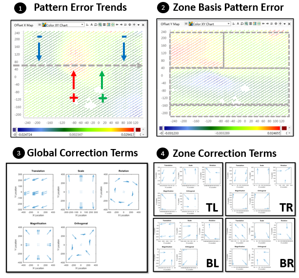
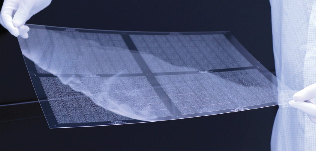
The benefits of glass carriers, however, come with several challenges, none of which should come as a surprise to anyone who has ever handled glass, whether in the fab or at home. Glass is fragile and, as such, is prone to surface defects, subsurface inclusions, and residual stress. Each of these can negatively impact die attachment quality, interconnect reliability, and die yield.

Let’s take a look at three major yield-killing culprits.


Surface defects such as particles, pits, and scratches are among the most common issues and may occur during glass carrier handling and processing, compromising the structural integrity and performance of advanced packaging assemblies (Figure 1)Particles can interfere with the bonding process, leading to poor adhesion or electrical discontinuities, while pits and scratches can propagate stress points that weaken the carrier during thermal cycling or molding. 

However, subsurface inclusions and organic contamination, which are often introduced during reclaim or cleaning, pose more critical challenges. Inclusions within the glass can create localized stress concentrations, while organic residues can reduce UV transmission and cause bonding failures. These contaminants are particularly problematic in high-density interconnect environments where optical clarity and surface purity are critical.

Figure 1: Common glass carrier defects

In addition to surface and subsurface defects, residual stress represents a concern. Over time, these stress points, manifesting during thermal processing or mechanical handling, can lead to cracks or delamination, undermining the thermo-mechanical integrity of the entire package.

These potential challenges are compounded each time a glass carrier is reused in an effort to reduce overall packaging costs. Fortunately, technologies have been developed to address this obstacle. These technologies integrate AI-driven defect classification, real-time analytics, and adaptive scanning modes to maintain throughput without sacrificing accuracy, enabling manufacturers to detect surface anomalies, subsurface inclusions, and stress-induced defects with unprecedented precision.

Enabling Defect-Free Glass Carriers

Today’s wafer-based inspection platforms utilize laser scatterometry and imaging techniques to inspect for nanometer sized defects on a variety of opaque and transparent/semi-transparent substrates. These substrates may be suitable for either R&D or high-volume advanced IC substrate (AICS) and fan-out panel level processing (FOPLP) environments. Proprietary inspection technology with multiple detection channels and advanced signal processing algorithms is applied to achieve accuracy and reliability in glass carrier inspection.

Figure 2: Results of top (blue) and bottom (red) defect mapping.

With each channel optimized to capture unique scattering and reflection signatures, the technology differentiates between surface and subsurface defects, as well as stress-related anomalies, with remarkable accuracy. Surface particles, scratches, pits, bumps, surface contamination, film or bulk wafer stress, voids/inclusions can be detected, measured, characterized, and imaged. One of the most significant capabilities of this technology is the ability to conduct simultaneous top, bottom, and internal defect mapping, a critical need for transparent and semi-transparent substrates where defects can occur across multiple planes (Figure 2).

Beyond defect detection, Angstrom-level film thickness measurement provides precise control over surface coatings and residual layers. This capability is particularly valuable in the glass reclaim process where even minor variations in film thickness can impact UV transmission and bonding performance. By enabling accurate defect detection and grading, only glass carriers meeting stringent quality standards are returned to production.

By introducing technologies that mitigate risks by providing comprehensive defect mapping and stress analysis, manufacturers are able to maintain the mechanical and thermal integrity required for next-generation devices. This capability is especially valuable in markets such as AI devices, high-performance computing, and automotive electronics where reliability is non-negotiable. With this combination of advanced optical technology and robust algorithmic analysis, manufacturers can successfully achieve higher yields, lower costs, and greater confidence in their packaging processes.

Conclusion

As packaging complexity grows and the use of glass carriers increases, inspection systems that combine multi-depth defect mapping and stress analysis will become indispensable for ensuring yield and reliability in AI and HPC devices. With the explosive growth in AI-driven data centers and advanced packaging architectures, manufacturers need solutions that combine accuracy, speed, and cost efficiency. The laser-based wafer inspection technology discussed in this blog meets several glass carrier challenges head-on while enabling advanced packaging houses to maintain defect-free glass carriers in support of next-generation advanced packaging.

The future of glass carriers is clear: with the right technologies at the ready, manufacturers have the tools and the means to meet the growing needs of the AI and HPC markets.

Biography

Jason Lin is Director of Product Marketing at Onto Innovation.

You Have
a Challenge? Let’s talk.

We’d love to connect with you.

Looking to learn more about our innovative solutions and capabilities? Our team of experts is ready to assist you. Reach out today and let’s starts a conversation about how we can help you achieve your goals.

Let’s Talk

"*" indicates required fields

This field is for validation purposes and should be left unchanged.

FAaST® CV/IV System

The FAaST system is a versatile, non-contact electrical metrology platform, with an option to combine micro and macro corona-Kelvin technologies together with digital surface photovoltage (SPV). It enables high-resolution dielectric and interface measurements across a wide range of dielectric materials, supporting both R&D and high volume manufacturing.

faast_350withmonitor-NEW

Product Overview

The primary application of non-contact CV metrology is monitoring dielectric properties during IC manufacturing. Unlike conventional electrical measurements, it requires no sample preparation, eliminating the need for MOS capacitor structures. This reduces metrology cost and enables fast data feedback in both R&D and manufacturing environments. 

The corona-Kelvin method uses a corona discharge in air to deposit an electric charge (DQC) on the wafer surface. A vibrating Kelvin-probe then measures the resulting surface voltage (V), enabling determination of the differential capacitance (C= DQC/DV). By monitoring surface voltage in both dark and illuminated conditions, the system separates two key components: dielectric voltage (VD) and semiconductor surface potential (VSB), enabling determination of flat band voltage (VFB). 

Analysis of the resulting charge-voltage data yields electrical parameters, including trap density (Dit)flat band voltage (Vfb)dielectric charge (Qtot), dielectric capacitance (CD), Equivalent Oxide Thickness (EOT)leakage current, and tunneling characteristics. 

Applications

  • Plasma damage monitoring
  • Residual charge and non-visual defect inspection
  • Diffusion furnace oxide and interface characterization
  • High-K and low-K dielectric capacitance
  • Mobile ion mapping
  • Charge trapping and hysteresis
Related Products
View all
FAaST® Digital SPV _feat

FAaST® Digital SPV System 

The FAaST Digital Surface PhotoVoltage (SPV) system delivers leading sensitivity for silicon wafer contamination control, rapidly mapping minority carrier diffusion length and detecting economically impactful iron (Fe) in minutes.
View Product
CnCV® System _feat

CnCV® System 

The CnCV (corona non-contact capacitance voltage) system is a powerful non-contact electrical metrology platform for dopant profiling and electrical defect mapping in wide bandgap (WBG) semiconductors.
View Product
Related Insights & Resources
View all

No items found.

Do you have a FAaST CV/IV system question? Let’s talk!

As your partner for innovative solutions, we’re always here for you.

Discover how our cutting-edge semiconductor solutions are engineered to meet your most complex challenges: delivering performance, reliability and innovation where it matters most.

Let’s Talk

"*" indicates required fields

This field is for validation purposes and should be left unchanged.

JetStep® X500 System

The JetStep X500 system is designed to provide AICS and OSAT manufacturers with a high-volume manufacturing lithography solution for heterogeneous integration. The JetStep X500 system exposes panel-type substrates made of CCL, FR4, composite, glass or other materials.

JetStep® X500 System

Product Overview

The JetStep X500 panel lithography system is optimized for high volume manufacturing of high-end AICS and other advanced packaging panel applications. As we approach the limits of Moore’s law, the JetStep X500 system addresses the need for extremely large packages integrating multi-node chips, or “chiplets,” enhancing functionality, speed, I/O count and reducing power consumption for server farms, AI, and mobile applications. The JetStep X500 system features the industry’s largest exposure field , fine line RDL resolution with large depth of focus (DOF), excellent overlay accuracy, and automatic magnification compensation with independent x and y magnification adjustment. The JetStep X500 system handles a large range of substrate thicknesses with high levels of warp, offering unique imaging parameter control to compensate for panel distortion. Additionally, it can run highly warped substrates with an edge clamping option and provides real-time autofocus at every exposure site to compensate for challenging topography.

Applications

  • AICS
  • Fan-out panel level packaging (FOPLP)
  • Large package formats, exposed without stitching
  • Large interposers
  • Redistribution layer (RDL) / underbump metallization (UBM)
  • Vias in photo imageable dielectric (PID)

Featured Markets

deco-bg-1 deco-bg-2
Related Products
View all
jetsetps3500_feat

JetStep® S3500 System

Advanced packaging lithography system designed for fan-out panel level packaging, accommodating substrates up to 720mm x 600mm
View Product
stepfast_feat

StepFAST® Software

An advanced feed-forward lithography software solution for fan-out panel level packaging that enhances yield and throughput by correcting die placement errors through external measurements, predictive analytics and adaptive shot control.
View Product
Related Insights & Resources
View all
early zone

Early Zone Correction for Enhanced Overlay Precision in Next-Generation FOPLP Lithography

Learn more
Yield Prediction Technology

Yield Prediction Technology: A Game Changer for Cutting Costs and Reducing Ramp Time in FOPLP Lithography

Learn more
roadmap

The Innovations Driving the Advanced Packaging Roadmap, Part 1

Learn more
Default product image

Onto Innovation’s PACE Partners Talk About Collaborating on Panel-Level Packaging

Learn more
20240930_Onto_00461

Picking up the Pace of Panel-level Advanced Packaging at Onto Innovation

Learn more
Overlay Optimization in Advanced IC Sub

Overlay Optimization In Advanced IC Substrates

Learn more
Picture1_240318_155910

How AI is Helping Optimize AI Chip Production

Learn more
glass-substrate_240212_181245

The Great Lithography Debate: Copper Clad Laminate or Glass Substrates?

Learn more
chip-sacle-review

Optimizing Advanced IC Substrates (AICS) for PLP

Learn more
Default product image

Total Overlay With Multiple RDLs with Keith Best

Learn more
glass-substrate

The Glass Substrate Question: When Will It Replace Copper Clad Laminate?

Learn more
overlay

Addressing Copper Clad Laminate Processing Distortion Using Overlay Corrections

Learn more
Address-image

Addressing Total Overlay Drift In Advanced IC Substrate (AICS) Packaging

Learn more
Correcting-Overlay

Heterogeneous Integration: Correcting Overlay Errors On Advanced Integrated Circuit Substrates (AICS)

Learn more
Het-Int

Heterogeneous Integration: Exposing Large Panels with Fewer Shots

Learn more
SC-Sept

‘XL’ Fine Resolution Large Field Lithography Dramatically Cuts FOPLP Pattern Distortion

Learn more
ECTC-2022-Image

Analysis of Pattern Distortion by Panel Deformation and Addressing it by Using Extremely Large Exposure Field Fine-Resolution Lithography

Learn more
fig-5_220126_110608

Outlier Control Technology and Feedforward Lithography Can Boost FOPLP Yield

Learn more
fine-res-litho

Large-field, Fine-resolution Lithography Enables Next-generation Panel-level Packaging

Learn more
Extremely-large

Extremely Large Exposure Field With Fine Resolution Lithography Technology To Enable Next Generation Panel Level Advanced Packaging

Learn more
Picture1_210722_090506

Advanced Outlier Die Control Technology in Fan-Out Panel Level Packaging Using Feedforward Lithography

Learn more
overlay-results

Adaptive Shot Technology To Address Severe Lithography Challenges For Advanced FOPLP

Learn more

Do you have a JetStep X500 question? Let’s talk!

As your partner for innovative solutions, we’re always here for you.

Discover how our cutting-edge semiconductor solutions are engineered to meet your most complex challenges: delivering performance, reliability and innovation where it matters most.

Let’s Talk

"*" indicates required fields

This field is for validation purposes and should be left unchanged.

JetStep® S3500 System

The JetStep S3500 system is designed to provide OSATS with a high-volume manufacturing advanced packaging lithography solution. For substrates up to 720mm x 600mm, it supports fan-out panel level packaging.

JetStep® S3500 System

Product Overview

The JetStep S3500 panel lithography system is specifically designed for advanced packaging panel production. As fan-out packages increase in size and complexity, requiring panel substrates instead of wafers, the JetStep S3500 system addresses these challenges with advanced features. It handles die shift caused by placement accuracy errors, CTE mismatch and panel warpage. The system incorporates a large exposure field (59.4 x 59.4mm) with resolution capability to 2/2 L/S and options for increased resolution to 1/1. In addition, it supports multiple exposure wavelengths, ideal for process development with new photosensitive polymers. Application-specific options include warped panel handling, “on-the-fly” optical focus, and die shift correction (StepFAST Solution), helping to ensure precise and reliable panel-level packaging.

Applications

  • Fan-out panel level packaging (FOPLP)
  • Interposers
  • Photo imageable Dielectric (PID) vias
  • Redistribution lines (RDL) / Under bump metallization (UBM)
  • Non-standard substrates

Featured Markets

Related Products
View all
jetstepx500_feat

JetStep® X500 System

Designed for advanced integrated circuit substrates (AICS) and other advanced packaging manufacturing applications, incorporating a 250mm x 250mm large field exposure area achieving 3μm L/S resolution with a large depth of focus.
View Product
stepfast_feat

StepFAST® Software

An advanced feed-forward lithography software solution for fan-out panel level packaging that enhances yield and throughput by correcting die placement errors through external measurements, predictive analytics and adaptive shot control.
View Product
Related Insights & Resources
View all
glass-substrate_240212_181245

The Great Lithography Debate: Copper Clad Laminate or Glass Substrates?

Learn more
overlay-results

Adaptive Shot Technology To Address Severe Lithography Challenges For Advanced FOPLP

Learn more

Do you have a JetStep S3500 question? Let’s talk!

As your partner for innovative solutions, we’re always here for you.

Discover how our cutting-edge semiconductor solutions are engineered to meet your most complex challenges: delivering performance, reliability and innovation where it matters most.

Let’s Talk

"*" indicates required fields

This field is for validation purposes and should be left unchanged.

PrimaScan™ P System

The PrimaScan P System provides all-surface defect and contamination inspection with imaging capability for glass panel substrates.

PrimaScan™ P System

Product Overview

As panel-level-packaging (PLP) transition from copper-clad laminates (CCL) to glass, the industry must adapt to ensure starting substrates are free of killer defects and contamination or latent defects that may result in yield loss or scrapped panels at later stages in the process flow. The PrimaScan P system is specifically designed to address incoming glass panel quality control for both the advanced IC substrate (AICS) and fan-out panel level processing (FOPLP) segments.

The PrimaScan P system delivers unique laser-based scanning and imaging via proprietary optics and sensing technologies for the reliable inspection of nanometer sized defects for either R&D or high-volume manufacturing environments. Utilizing multiple channel inspection technologies, the system can detect, measure and image surface particles, scratches, pits, surface contamination, stains, film or bulk panel stress, voids/inclusions, including chips and cracks at the edge of the panel.

Applications

  • Incoming unpatterned glass panel quality inspection
  • Blanket photoresist, dielectric or metallic coated panels
  • Buried defects and voids in transparent and semi-transparent blanket films
  • Across panel stress and induced point stress
Related Products
View all
primascan_feat

PrimaScan™ System

All-surface defect and contamination inspection for unpatterned wafer and blanket films, with imaging capability for opaque, transparent and semi-transparent wafers, reticles and piece parts.
View Product
primascan r&d_feat

PrimaScan™ R&D System

All-surface defect and contamination inspection for unpatterned wafer and blanket films, with imaging capability for opaque, transparent and semi-transparent wafers, reticles and piece parts.
View Product

Do you have a PrimaScan P question? Let’s talk!

As your partner for innovative solutions, we’re always here for you.

Discover how our cutting-edge semiconductor solutions are engineered to meet your most complex challenges: delivering performance, reliability and innovation where it matters most.

Let’s Talk

"*" indicates required fields

This field is for validation purposes and should be left unchanged.

Firefly® G3 System

The Firefly G3 system provides automated inspection and 3D metrology for advanced IC substrates and panel level packaging, delivering high resolution and productivity for demanding applications like high-performance computing (HPC), artificial intelligence (AI), cloud computing and machine/deep learning.

Firefly® G3 System

Product Overview

The Firefly G3 platform offers multiple imaging modes, including Onto Innovation’s patented Clearfind® Technology, a technique to detect residue defects on metal and metal defects on organic layers. The combination of high sensitivity inspection, 2D/3D metrology and on tool color image capture capability in a single platform reduces capital investment requirements and provides a reliable pathway for panel-based process applications that require high I/O counts and multiple-chip integration.

Integration with Onto Innovation’s Discover® Defect and TrueADC® software quickly turns defect data into actionable process control, improves defect classification and reduces manual review. It enables our customers to develop, learn and analyze new processes reliably while significantly improving their product delivery time to market.

Applications

  • Advanced IC Substrates (AICS): CCL and Glass
  • Fan-out Panel Level Packaging (FOPLP)
  • Interposers
  • Embedded Die substrates/ Interposer
  • 2.5D/3D integration
Related Products
View all
discoverdefect_feat

Discover® Defect Software

Integrated defect management system that works seamlessly with Onto tools and your entire enterprise, bringing data together for greater visibility and cleaner operation.
View Product
discoverreview_feat

Discover® Review Software

Your smart factory’s human classification interface.
View Product
stepfast_feat

StepFAST® Software

An advanced feed-forward lithography software solution for fan-out panel level packaging that enhances yield and throughput by correcting die placement errors through external measurements, predictive analytics and adaptive shot control.
View Product
Related Insights & Resources
View all
intellignet innovation oct 2025 fig 4

Through the Glass: Why the Rapid Development of TGV Demands Rigorous Analysis

Learn more
roadmap

The Innovations Driving the Advanced Packaging Roadmap, Part 1

Learn more
Default product image

Onto Innovation’s PACE Partners Talk About Collaborating on Panel-Level Packaging

Learn more
20240930_Onto_00461

Picking up the Pace of Panel-level Advanced Packaging at Onto Innovation

Learn more
the-long-climb

The Long Climb: Bringing Through Glass Vias (TGV) to High-Volume Manufacturing

Learn more
chip-scale-review

Using 2D/3D Technology to Overcome Challenges of Large-Area Panel Inspection and Metrology

Learn more
Picture1_240318_155910

How AI is Helping Optimize AI Chip Production

Learn more
chip-sacle-review

Optimizing Advanced IC Substrates (AICS) for PLP

Learn more
glass-substrate

The Glass Substrate Question: When Will It Replace Copper Clad Laminate?

Learn more
overlay

Addressing Copper Clad Laminate Processing Distortion Using Overlay Corrections

Learn more
illumina

Illumination Inspection Technology for Defect Detection on Advanced IC Substrates

Learn more
Address-image

Addressing Total Overlay Drift In Advanced IC Substrate (AICS) Packaging

Learn more
Default product image

Nip the Defect in the Bud: Using an external inspection system and FDC software increases ABF substrate yield

Learn more
fig-5_220126_110608

Outlier Control Technology and Feedforward Lithography Can Boost FOPLP Yield

Learn more
Picture1_210722_090506

Advanced Outlier Die Control Technology in Fan-Out Panel Level Packaging Using Feedforward Lithography

Learn more
defects-on-600mm

Revealing Invisible Defects on Large 600mm Panels

Learn more
overlay-results

Adaptive Shot Technology To Address Severe Lithography Challenges For Advanced FOPLP

Learn more

Do you have a Firefly G3 system question? Let’s talk!

As your partner for innovative solutions, we’re always here for you.

Discover how our cutting-edge semiconductor solutions are engineered to meet your most complex challenges: delivering performance, reliability and innovation where it matters most.

Let’s Talk

"*" indicates required fields

This field is for validation purposes and should be left unchanged.