
PrimaScan™ System
All-surface defect and contamination inspection for unpatterned wafer and blanket films, with imaging capability for opaque, transparent and semi-transparent wafers, reticles and piece parts.

Specialty devices are the unsung heroes of modern life. For many in the semiconductor industry today, the spotlight is on the SiC and GaN power devices used in automotive, green energy, fast-charge consumer electronics (CE), and high-performance computing (HPC) applications.

The Celero PL system is designed for subsurface defect inspection and classification for silicon carbide (SiC) and gallium nitride (GaN) based wafers and compound semiconductor materials.
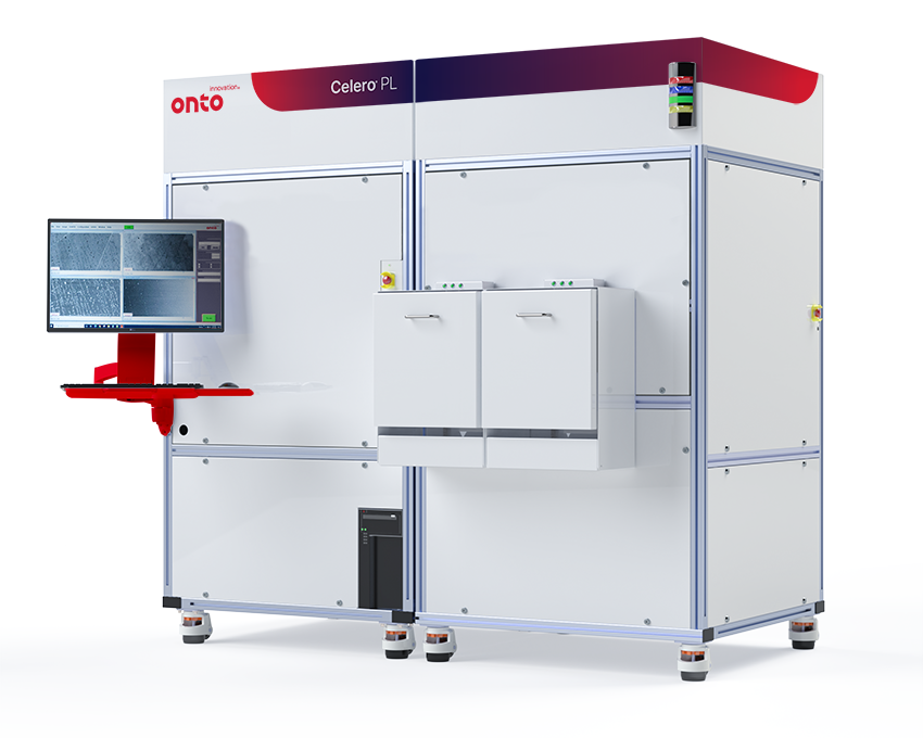
The Celero PL system utilizes a laser-based phase detection and imaging capability that leverages custom optics and image processing algorithms to enable best in class throughput and sensitivity for silicon carbide and gallium nitride-based materials on 100mm to 300mm wafer sizes. Leveraging multiple light sources and sensor channels, the system can detect, measure and image a broad variety of subsurface crystalline defects, associated with bulk wafers and epitaxial layers, surface particles, scratches, pits, surface contamination, stains, point or bulk wafer stress, voids/inclusions, including chips and cracks at the edge of the wafer.


As your partner for innovative solutions, we’re always here for you.
Discover how our cutting-edge semiconductor solutions are engineered to meet your most complex challenges: delivering performance, reliability and innovation where it matters most.
"*" indicates required fields
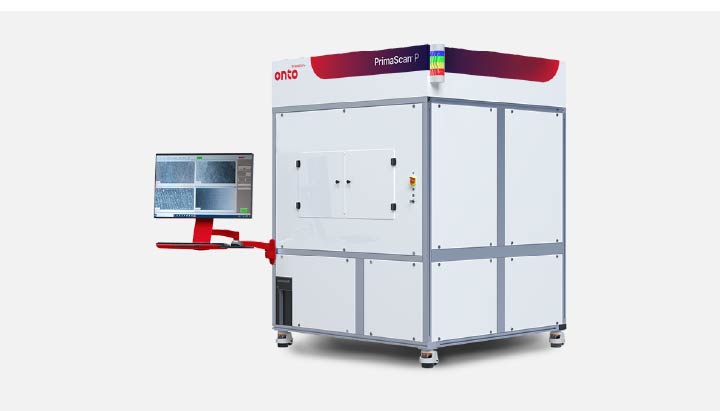
The PrimaScan P System provides all-surface defect and contamination inspection with imaging capability for glass panel substrates.
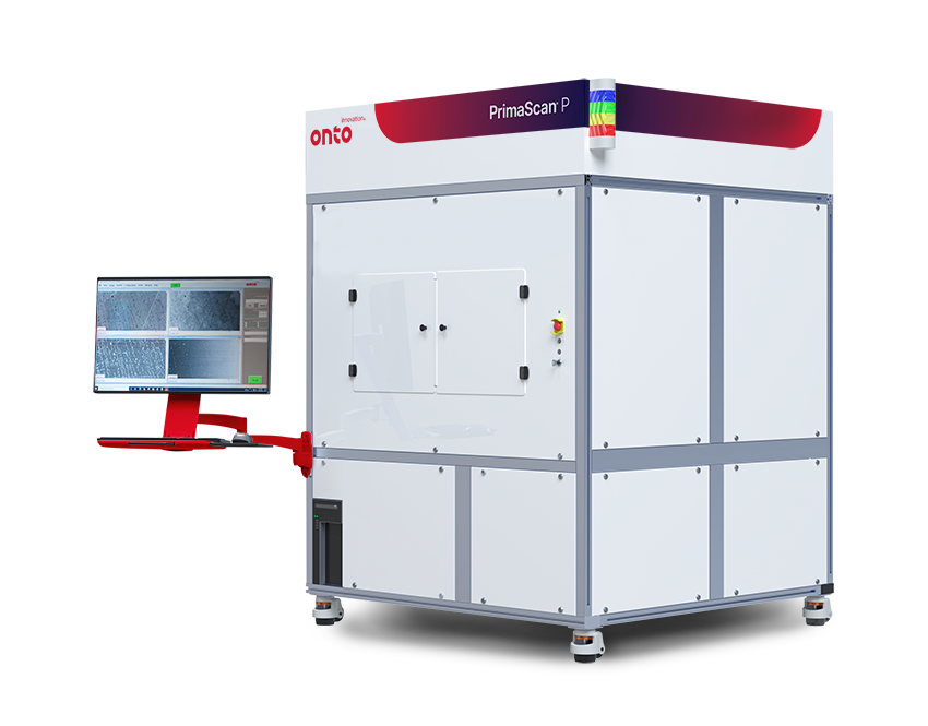
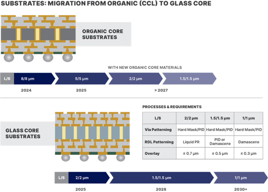
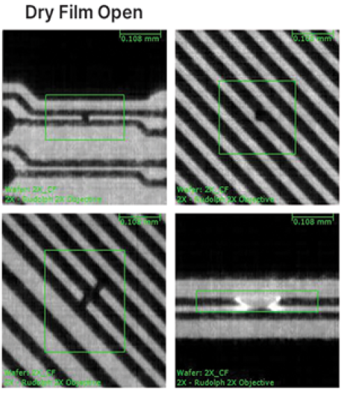
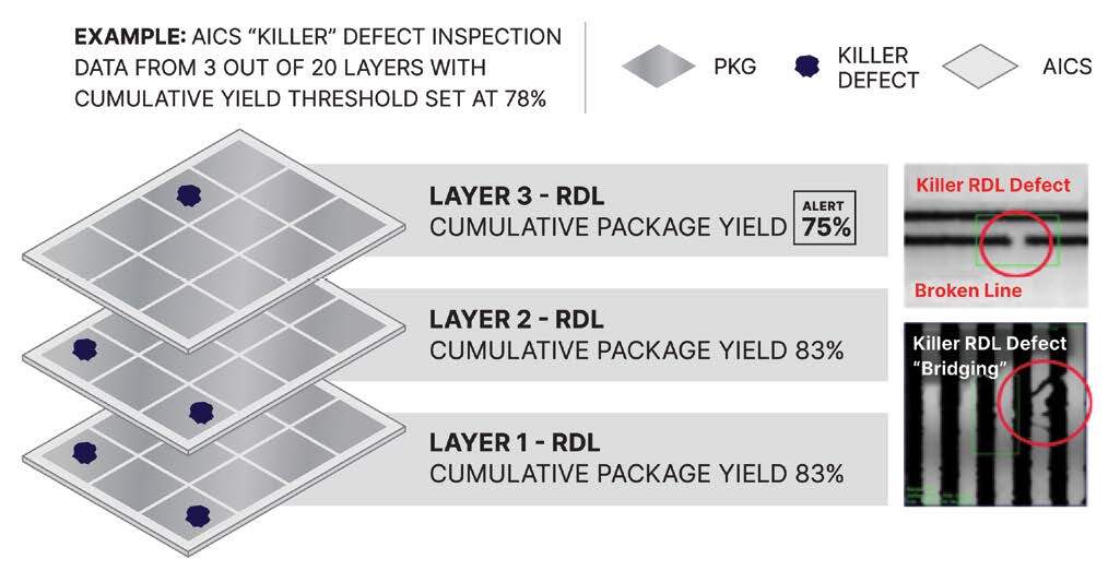
As panel-level-packaging (PLP) transition from copper-clad laminates (CCL) to glass, the industry must adapt to ensure starting substrates are free of killer defects and contamination or latent defects that may result in yield loss or scrapped panels at later stages in the process flow. The PrimaScan P system is specifically designed to address incoming glass panel quality control for both the advanced IC substrate (AICS) and fan-out panel level processing (FOPLP) segments.
The PrimaScan P system delivers unique laser-based scanning and imaging via proprietary optics and sensing technologies for the reliable inspection of nanometer sized defects for either R&D or high-volume manufacturing environments. Utilizing multiple channel inspection technologies, the system can detect, measure and image surface particles, scratches, pits, surface contamination, stains, film or bulk panel stress, voids/inclusions, including chips and cracks at the edge of the panel.
As your partner for innovative solutions, we’re always here for you.
Discover how our cutting-edge semiconductor solutions are engineered to meet your most complex challenges: delivering performance, reliability and innovation where it matters most.
"*" indicates required fields
The PrimaScan R&D System is a stand-alone, manual load version of the PrimaScan automated wafer defect and contamination inspection system that has been specifically designed with R&D and lab environments in mind.
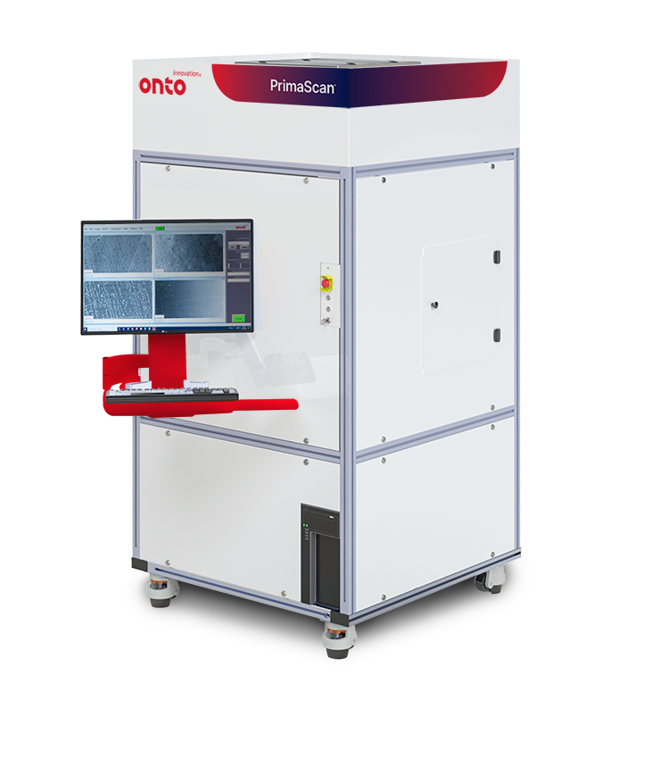
The PrimaScan R&D system offers a smaller spot size and higher pixel resolution than its high volume production counterpart tools. The flexibility in sample handling options combined with the multiple sensing channels and higher resolution imaging makes this the ideal tool for R&D and lab environments. Similar to the other tools in the PrimaScan line, the PrimaScan R&D system offers reliable inspection of nanometer sized defects on a variety of opaque and transparent/semi-transparent substrates and samples suitable for either R&D or lab environments. The system can detect, measure, characterize and image surface particles, scratches, pits, bumps, surface contamination, film or bulk wafer stress, voids/inclusions, including chips and cracks at the wafer edge.
Designed with versatility in mind the PrimaScan R&D system can handle a variety of wafer sizes and substrate types including film frame, photomask and sample tray.
As your partner for innovative solutions, we’re always here for you.
Discover how our cutting-edge semiconductor solutions are engineered to meet your most complex challenges: delivering performance, reliability and innovation where it matters most.
"*" indicates required fields
The EB40 Module combines edge and backside inspection into one tool with the option to be paired with an inspection system to provide a high throughput all surface inspection solution.
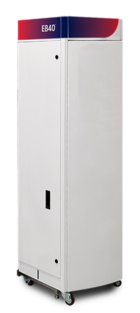
The Class 1 certified EB40 module offers combined edge and backside inspection and is also available as separate edge (E40) and backside (B40) modules. These modules provide brightfield and darkfield inspection to detect defects on the entire bevel and backside, covering Zone 1 to Zone 5. This enables faster root-cause analysis of defects that can migrate to the wafer interior, impacting die yield.
The EB40 module captures defect images on the fly, creates whole-wafer composite images, and integrates with SEM bevel review. All inspection and metrology results, including defect, whole wafer and SEM images can be analyzed together in a single database using Discover Defect software. Correlating EBR metrology with defectivity data, SEM data and micro-inspection results is just the beginning of what Discover software can do. In addition to advanced on-tool defect binning, real-time edge ADC classification can be assigned to defects prior to manual offline review using Discover Review software.


As your partner for innovative solutions, we’re always here for you.
Discover how our cutting-edge semiconductor solutions are engineered to meet your most complex challenges: delivering performance, reliability and innovation where it matters most.
"*" indicates required fields
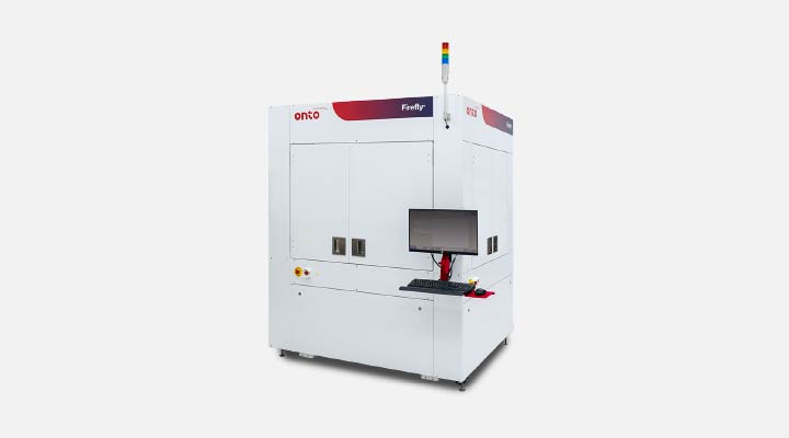
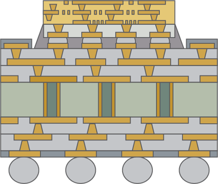
The Firefly G3 system provides automated inspection and 3D metrology for advanced IC substrates and panel level packaging, delivering high resolution and productivity for demanding applications like high-performance computing (HPC), artificial intelligence (AI), cloud computing and machine/deep learning.
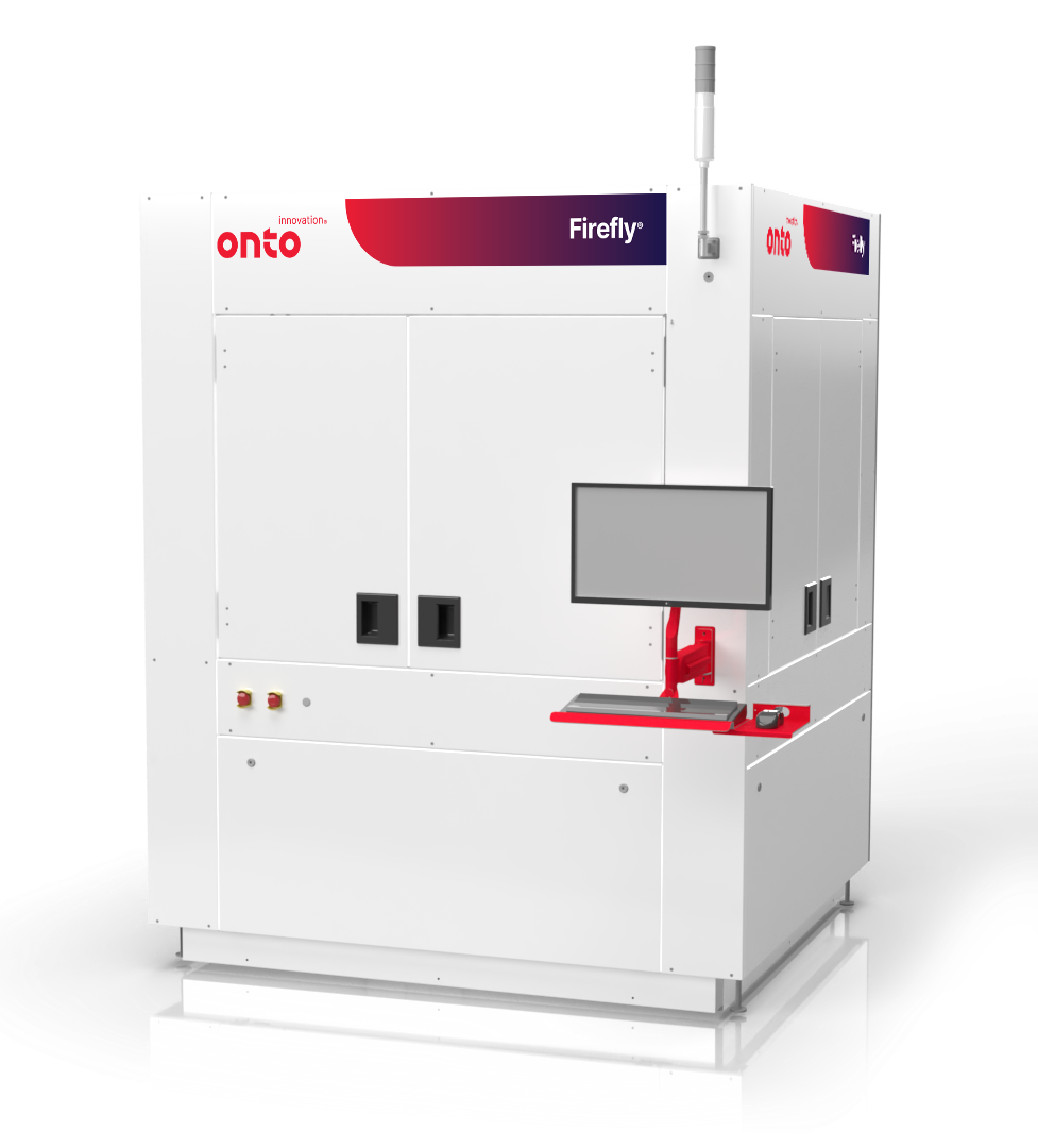
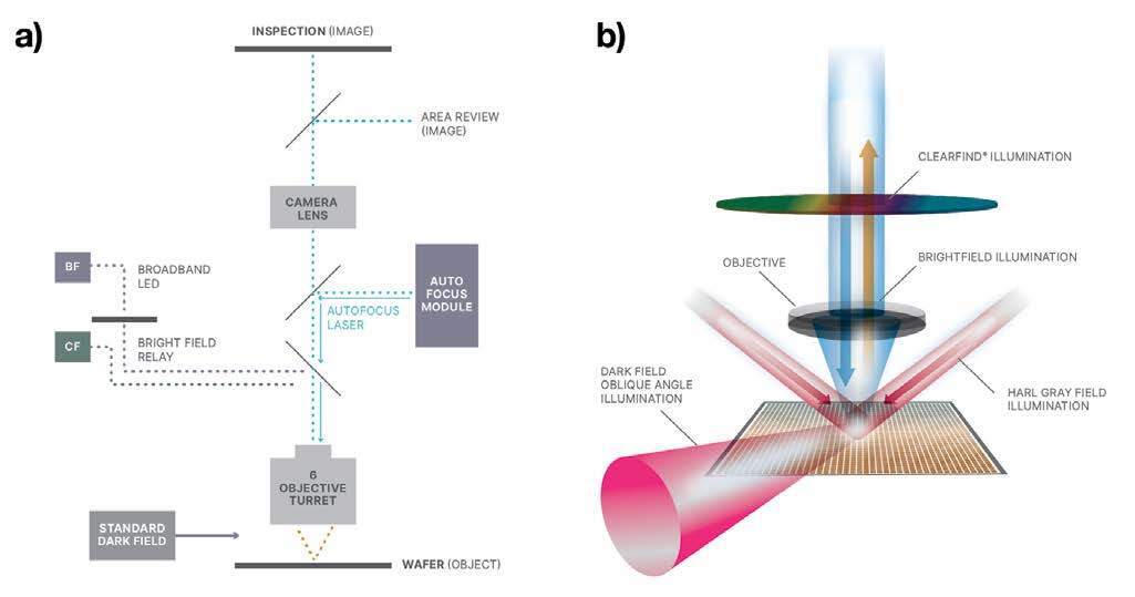
The Firefly G3 platform offers multiple imaging modes, including Onto Innovation’s patented Clearfind® Technology, a technique to detect residue defects on metal and metal defects on organic layers. The combination of high sensitivity inspection, 2D/3D metrology and on tool color image capture capability in a single platform reduces capital investment requirements and provides a reliable pathway for panel-based process applications that require high I/O counts and multiple-chip integration.
Integration with Onto Innovation’s Discover® Defect and TrueADC® software quickly turns defect data into actionable process control, improves defect classification and reduces manual review. It enables our customers to develop, learn and analyze new processes reliably while significantly improving their product delivery time to market.
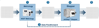
Die shift on reconstituted panels can significantly impact both productivity and yield. To address this challenge, we use a parallel die placement measurement process and advanced analytics to provide a means to balance productivity against yield. Our integrated lithography cell, featuring Firefly inspection, StepFAST software, and JetStep Lithography, delivers industry-leading throughput and yield for fan-out panel level packaging.
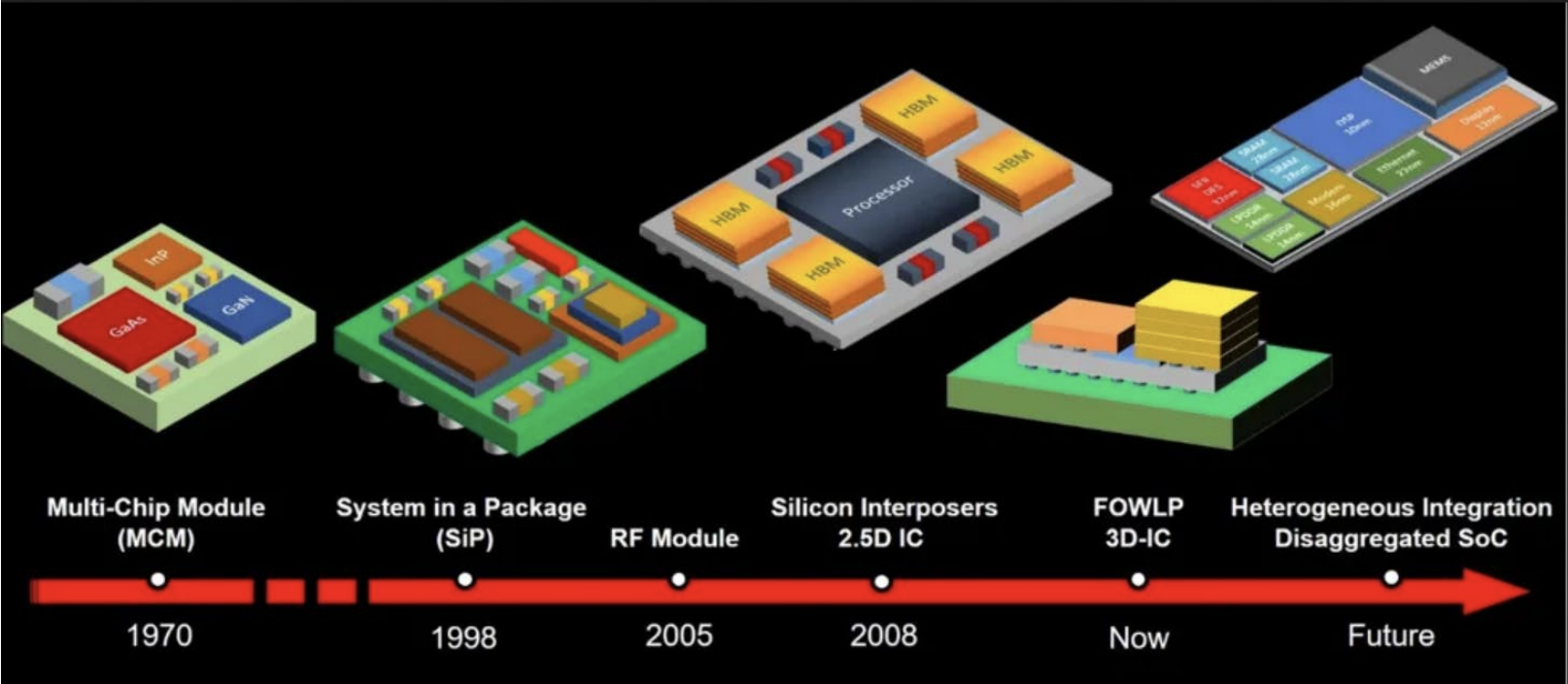
It is well understood that advanced packaging applications require high performance, low cost, increased functionality and improved reliability that 2.5D and 3D packaging solutions provide. Fan-out panel-level packaging (FOPLP) is one of the technologies that has the potential to meet these packaging requirements.
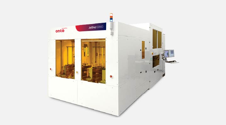
The JetStep S3500 system is designed to provide OSATS with a high-volume manufacturing advanced packaging lithography solution. For substrates up to 720mm x 600mm, it supports fan-out panel level packaging.
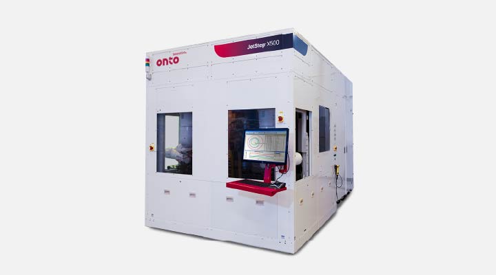
The JetStep X500 system is designed to provide AICS and OSAT manufacturers with a high-volume manufacturing lithography solution for heterogeneous integration. The JetStep X500 system exposes panel-type substrates made of CCL, FR4, composite, glass or other materials.
The Firefly G3 system provides automated inspection and 3D metrology for advanced IC substrates and panel level packaging, delivering high resolution and productivity for demanding applications like high-performance computing (HPC), artificial intelligence (AI), cloud computing and machine/deep learning.

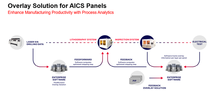
An advanced feed-forward lithography software solution for fan-out panel level packaging that enhances yield and throughput by correcting die placement errors through external measurements, predictive analytics and adaptive shot control.
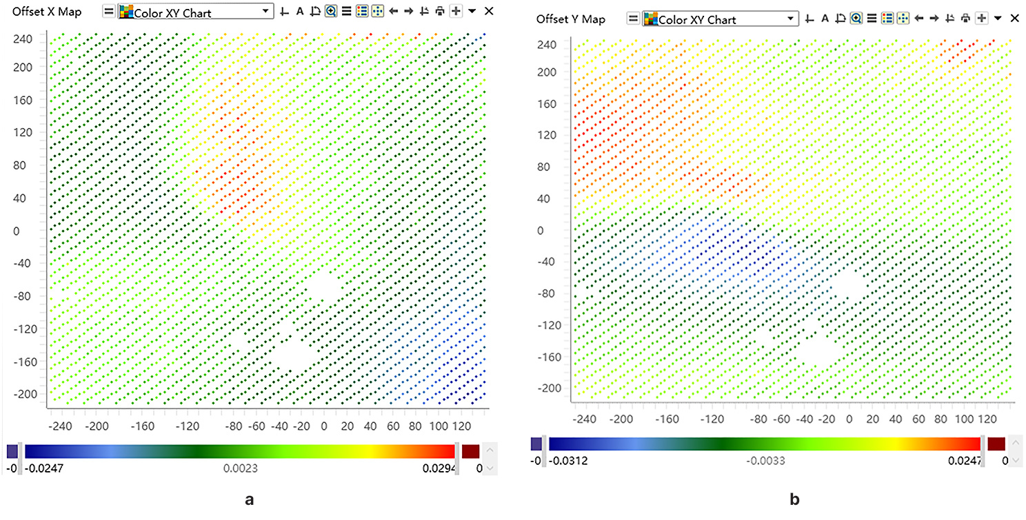
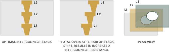
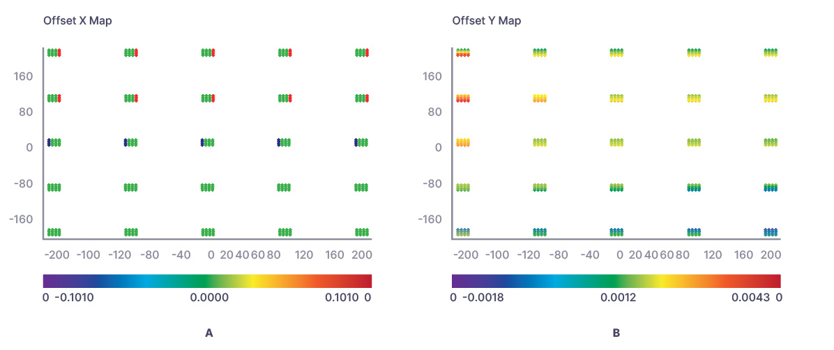
During the processing of organic (CCL) advanced IC substrates (AICS) the substrates become distorted which impacts the overlay of Via to RDL pad structures. To solve this problem, the stepper must adjust the alignment solution to match the previous layer’s distortion by measuring the overlay. Proprietary software provides the user with the ability to adjust each zone of the AICS with independent offsets.
The growing demand for heterogeneous integration is driven by the 5G market. This includes smartphones, data centers, servers, high-performance computing (HPC), artificial intelligence (AI) and internet of things (IoT) applications. Next generation packaging technologies require tighter overlay to accommodate larger package sizes with fine-pitch chip interconnects on large-format flexible panels.
Designed for advanced IC substrates (AICS), it incorporates a large field exposure area with a large depth of focus. Proprietary software enables independent zone offset adjustments across the AICS.
The Firefly G3 system provides automated inspection and 3D metrology for advanced IC substrates and panel level packaging, delivering high resolution and productivity for demanding applications like high-performance computing (HPC), artificial intelligence (AI), cloud computing and machine/deep learning.

As your partner for innovative solutions, we’re always here for you.
Discover how our cutting-edge semiconductor solutions are engineered to meet your most complex challenges: delivering performance, reliability and innovation where it matters most.
"*" indicates required fields
The Dragonfly G3 system is resetting the industry’s expectations for throughput, accuracy and reliability. Combining 2D and 3D technologies, the system detects yield-robbing defects and measures features critical for today’s semiconductor technologies
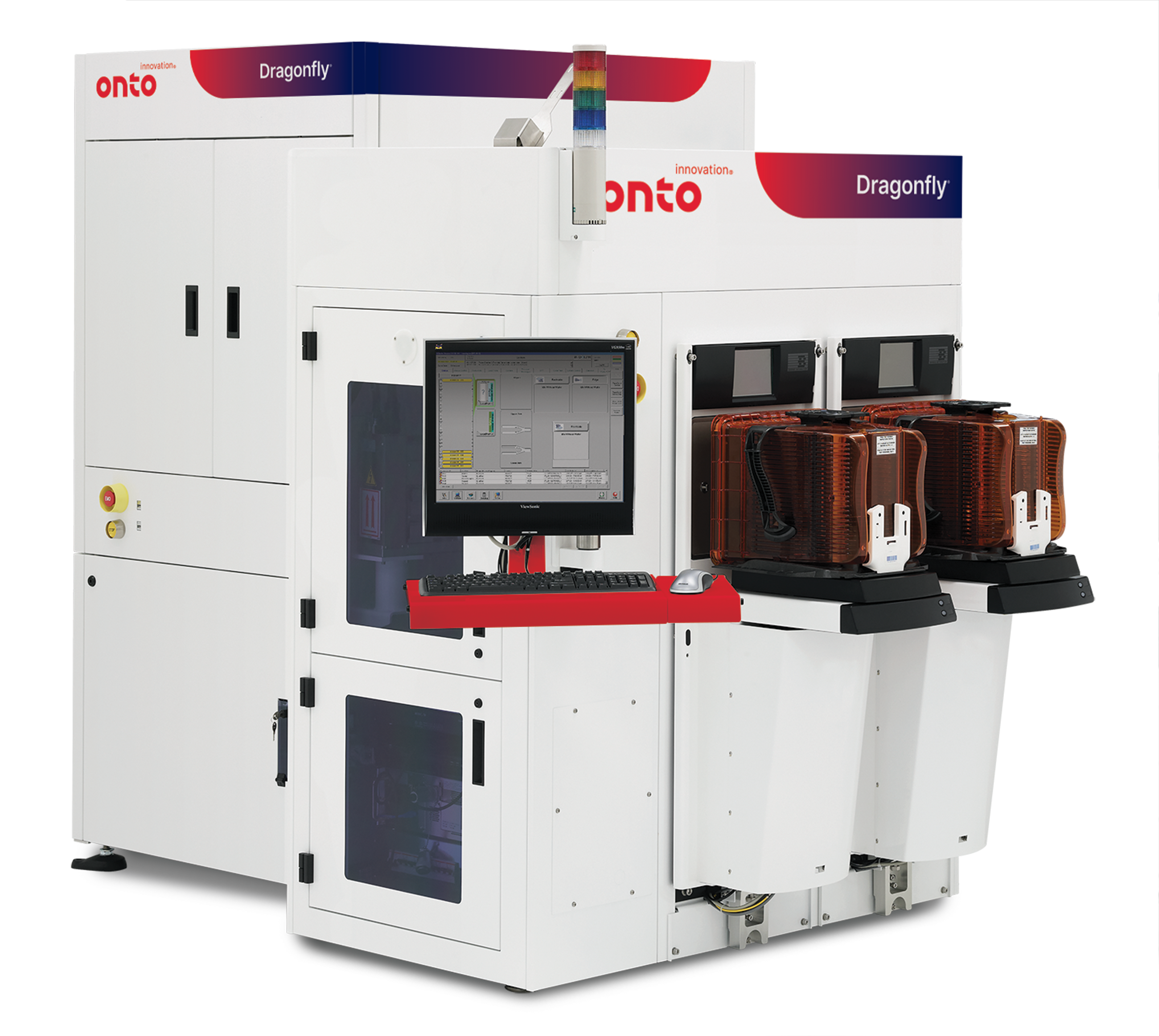
The Dragonfly G3 is a widely adopted pattern inspection system that utilizes line scan imaging technology to deliver fast, sub-micron defect detection for both R&D and high volume manufacturing environments. It features multiple illumination channels, including brightfield, darkfield, high-speed IR for embedded defects, and Clearfind® technology for detecting non-visual organic residues. Powered by modern machine learning algorithms, the Dragonfly G3 system offers a complete on-tool solution for defect detection, nuisance reduction and classification.
The system offers additional flexibility through the integration of multiple 3D metrology capabilities, including film thickness and structural profiling, and substrate thickness measurement. It features the latest 3Di™ technology, delivering and precise bump height metrology. The Dragonfly G3 system, with optional edge and backside inspection via the EB40 module, offers a comprehensive all-surface inspection solution for both front-end and back-end OQA.
Hybrid bonding enables ultra-dense 3D memory interconnects with up to 1,000x more connections than microbumps. Achieving high yield requires stringent process control, including monitoring topography and detecting particles, cracks and voids. Measuring dishing in copper pads provides valuable insight into surface conditions. Together, these process control insights contribute to improved device reliability and performance.

As demand grows for high-performance computing (HPC) and AI-driven applications, manufacturers are turning to hybrid bonding to enable the ultra-dense 3D integration required for next-generation chip architectures. This advanced packaging technology presents significant process challenges. Surface preparation must be precisely controlled to eliminate particles, excess recess, and copper pad dishing, all of which can compromise bond quality. During pre-annealing, particle-induced gaps and wide bonding gaps can prevent proper wafer contact. Post-annealing, the formation of dielectric and metal voids introduces further risks to electrical performance and long-term reliability.

The Iris S system is a versatile platform solution for the advanced packaging and specialty market, supporting 150mm, 200mm and 300mm wafers. It provides thin and thick film, OCD and wafer bow and film stress measurements.

The IMPULSE V system helps to advance CMP processing with enhanced wavefront technology and AI-driven analytics, delivering over 2X precision improvement and faster solutions, crucial for next-gen semiconductor manufacturing demands.
The Dragonfly G5 system is engineered for inline process control of leading-edge advanced packaging technologies. As the latest generation pattern inspection system in the Dragonfly series, it delivers unparalleled accuracy in detecting submicron defects and performing high-resolution 3D measurements.

The Aspect System is a revolutionary in-line, non-destructive infrared optical critical dimension (IRCD) system measuring Z-dimension profiling of high aspect ratio structures to enable critical process control. It meets the needs of leading-edge customers with its high speed and process coverage.


As your partner for innovative solutions, we’re always here for you.
Discover how our cutting-edge semiconductor solutions are engineered to meet your most complex challenges: delivering performance, reliability and innovation where it matters most.
"*" indicates required fields