
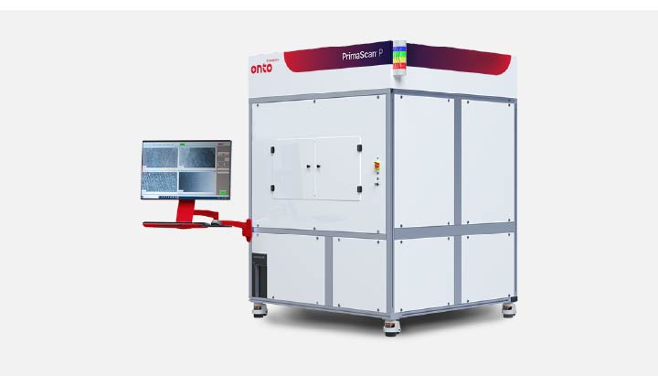
PrimaScan™ System
All-surface defect and contamination inspection for unpatterned wafer and blanket films, with imaging capability for opaque, transparent and semi-transparent wafers, reticles and piece parts.

If you’ve been following the evolution of advanced packaging, you know that the industry is pushing boundaries like never before. From high-performance computing to industry-upending AI devices, the demand for smaller, faster, and more powerful chips is driving innovation at every level.

The PrimaScan R&D System is a stand-alone, manual load version of the PrimaScan automated wafer defect and contamination inspection system that has been specifically designed with R&D and lab environments in mind.
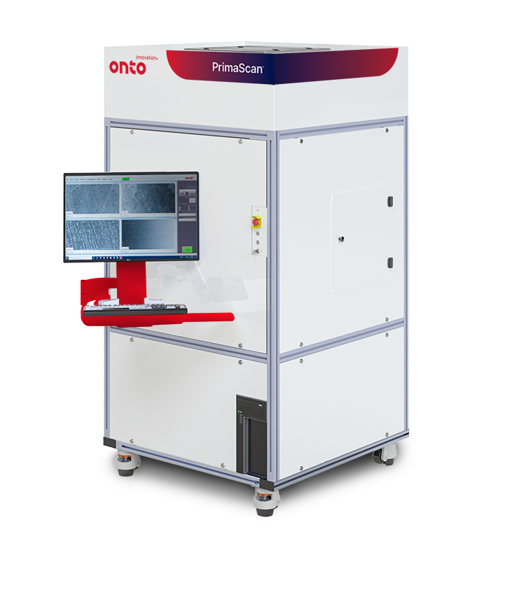
The PrimaScan R&D system offers a smaller spot size and higher pixel resolution than its high volume production counterpart tools. The flexibility in sample handling options combined with the multiple sensing channels and higher resolution imaging makes this the ideal tool for R&D and lab environments. Similar to the other tools in the PrimaScan line, the PrimaScan R&D system offers reliable inspection of nanometer sized defects on a variety of opaque and transparent/semi-transparent substrates and samples suitable for either R&D or lab environments. The system can detect, measure, characterize and image surface particles, scratches, pits, bumps, surface contamination, film or bulk wafer stress, voids/inclusions, including chips and cracks at the wafer edge.
Designed with versatility in mind the PrimaScan R&D system can handle a variety of wafer sizes and substrate types including film frame, photomask and sample tray.

As your partner for innovative solutions, we’re always here for you.
Discover how our cutting-edge semiconductor solutions are engineered to meet your most complex challenges: delivering performance, reliability and innovation where it matters most.
"*" indicates required fields
The EB40 Module combines edge and backside inspection into one tool with the option to be paired with an inspection system to provide a high throughput all surface inspection solution.
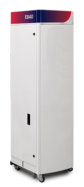
The Class 1 certified EB40 module offers combined edge and backside inspection and is also available as separate edge (E40) and backside (B40) modules. These modules provide brightfield and darkfield inspection to detect defects on the entire bevel and backside, covering Zone 1 to Zone 5. This enables faster root-cause analysis of defects that can migrate to the wafer interior, impacting die yield.
The EB40 module captures defect images on the fly, creates whole-wafer composite images, and integrates with SEM bevel review. All inspection and metrology results, including defect, whole wafer and SEM images can be analyzed together in a single database using Discover Defect software. Correlating EBR metrology with defectivity data, SEM data and micro-inspection results is just the beginning of what Discover software can do. In addition to advanced on-tool defect binning, real-time edge ADC classification can be assigned to defects prior to manual offline review using Discover Review software.


As your partner for innovative solutions, we’re always here for you.
Discover how our cutting-edge semiconductor solutions are engineered to meet your most complex challenges: delivering performance, reliability and innovation where it matters most.
"*" indicates required fields
The Dragonfly G3 system is resetting the industry’s expectations for throughput, accuracy and reliability. Combining 2D and 3D technologies, the system detects yield-robbing defects and measures features critical for today’s front-end and packaging technologies.
The Dragonfly G3 system utilizes line scan-based 2D imaging technology to provide fast, reliable inspection for sub-micron defects, meeting both current R&D and future production needs. It features multi-illumination channels, including brightfield/darkfield, high-speed IR for embedded defects and Clearfind® Technology for non-visual residue detection. For specialty markets like CMOS image sensors (CIS), it uses oblique angle illumination, sophisticated image processing and machine-learning algorithms to detect low contrast defects in the active pixel sensor area.
Optional 3D metrology sensors include the latest 3Di™ technology, delivering fast, precise bump height metrology. Discover Software visualizes the massive amounts of bump data, correlating process variations to improve yields. TrueADC software enables real time automatic classification of critical defects and reduces nuisance defects. The Dragonfly G3 system, with optional edge and backside inspection via the EB40 module, offers a comprehensive all-surface inspection solution for next generation technology challenges.
Hybrid bonding enables ultra-dense 3D memory interconnects with up to 1,000x more connections than microbumps. Achieving high yield requires stringent process control, including monitoring topography and detecting particles, cracks and voids. Measuring dishing in copper pads provides valuable insight into surface conditions. Together, these process control insights contribute to improved device reliability and performance.

As demand grows for high-performance computing (HPC) and AI-driven applications, manufacturers are turning to hybrid bonding to enable the ultra-dense 3D integration required for next-generation chip architectures. This advanced packaging technology presents significant process challenges. Surface preparation must be precisely controlled to eliminate particles, excess recess, and copper pad dishing, all of which can compromise bond quality. During pre-annealing, particle-induced gaps and wide bonding gaps can prevent proper wafer contact. Post-annealing, the formation of dielectric and metal voids introduces further risks to electrical performance and long-term reliability.

The Iris S system is a versatile platform solution for the advanced packaging and specialty market, supporting 150mm, 200mm and 300mm wafers. It provides thin and thick film, OCD and wafer bow and film stress measurements.

The IMPULSE V system helps to advance CMP processing with enhanced wavefront technology and AI-driven analytics, delivering over 2X precision improvement and faster solutions, crucial for next-gen semiconductor manufacturing demands.
The Dragonfly G3 system is resetting the industry’s expectations for throughput, accuracy and reliability. Combining 2D and 3D technologies, the system detects yield-robbing defects and measures features critical for today’s front-end and packaging technologies.

The Aspect System is a revolutionary in-line, non-destructive infrared optical critical dimension (IRCD) system measuring Z-dimension profiling of high aspect ratio structures to enable critical process control. It meets the needs of leading-edge customers with its high speed and process coverage.


As your partner for innovative solutions, we’re always here for you.
Discover how our cutting-edge semiconductor solutions are engineered to meet your most complex challenges: delivering performance, reliability and innovation where it matters most.
"*" indicates required fields
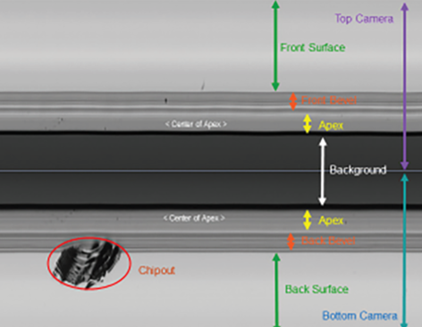
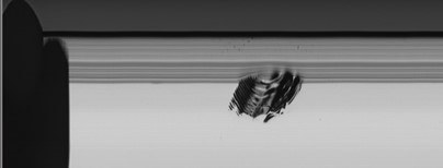
The NovusEdge G2 System offers fast, reliable edge, notch and backside inspection for 300mm unpatterned wafers, utilizing modular configurations.
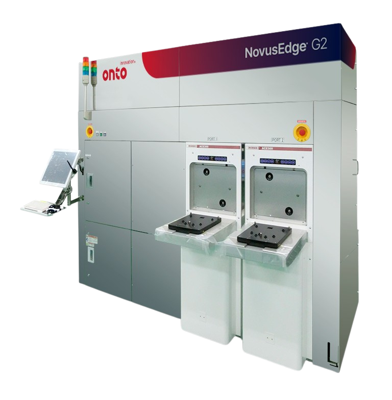
The NovusEdge G2 System provides high sensitivity inspection for the edge and backside of unpatterned wafers for current and advanced nodes. Configurable modules on the same automation platform increase throughput while maintaining a small footprint for improved cost of ownership. The edge-gripping handling solution for both automation platform and the inspection modules provide desired cleanliness required for manufacturing. Optional high-sensitivity notch inspection can be added. Defects are automatically classified and binned at run time to reduce manual review.
Designed as a multipurpose inspection and sorting system for end of line outgoing quality inspection of 300mm unpatterned wafers, the system identifies, inspects and sorts wafers according to recipes.
The NovusEdge G2 system offers higher sensitivity than the previous generation, with sub-micron resolution and increased throughput by over 15%. User interaction is simplified, and the new electrical design consumes less power.
As your partner for innovative solutions, we’re always here for you.
Discover how our cutting-edge semiconductor solutions are engineered to meet your most complex challenges: delivering performance, reliability and innovation where it matters most.
"*" indicates required fields
By Cheolkyu Kim, Onto Innovation, and Dae-Seo Park, Samsung Electronics Co., Ltd.
Picosecond ultrasonic technology can provide a metrology solution with excellent accuracy and gage capability for the control of interconnect processes in advanced packaging.
Looking back, 2024 will likely be remembered as a turning point for artificial intelligence (AI). Thanks to the spread of ChatGPT, Microsoft’s Copilot and other large language models, as well as various generative AI tools for video and images, AI has emerged as a tool used by millions of people every day. To create these new high performance AI devices, memory and process chips are packaged together to enable faster communication and lower power consumption. Such devices use advanced packaging technologies like heterogeneously integrated 2.5D and 3D structures.
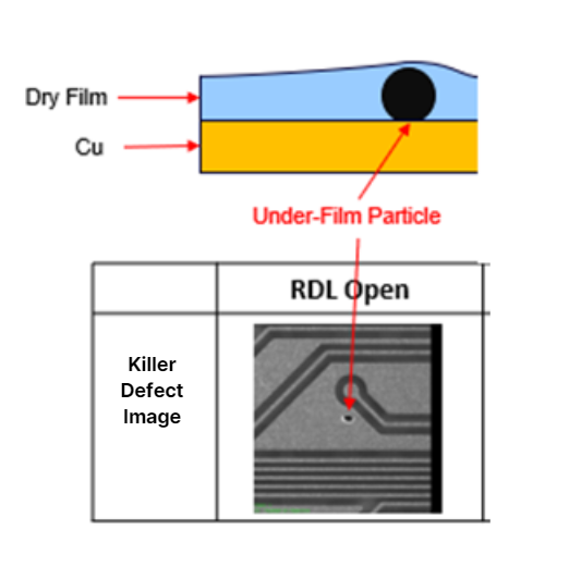
In these 2.5D and 3D structures, conventional memory chips are replaced with high bandwidth memory (HBM) and paired with a graphics processing unit (GPU). The HBM enables the higher data transfer rates needed to handle the significantly increased data processing generated by parallel computation with the GPU. In the latest generation HBM, eight to 12 DRAM chips are connected to each other vertically by through silicon vias (TSV) to form one HBM package. Then four to six HBM packages are connected, horizontally, with the GPU chip by redistribution layers (RDL) on a Si interposer. These new interconnected structures offer significantly improved computing power, latency and higher bandwidth for data transfer and low power consumption as required by AI computing.
In the case of RDL on a Si interposer, manufacturing multiple layers of RDL is required to handle high data transfer rates. As such, the manufacturing process is much more complex compared to the manufacturing process for more mature packages. Metals, mostly Cu, in RDL are typically deposited using the electroplating (EP) process. The thickness of the metals is affected by the geometric structure underneath, making thickness uniformity control very challenging. To meet the within wafer uniformity requirement for RDL impedance control, measuring and monitoring metal thickness directly on product wafers is crucial. As RDL lines shrink to 2µm or lower – the line/space (L/S) requirements of the most advanced packages – dimensional control is vital to device performance while process control itself becomes even more stringent.
After the final RDL layer on a Si interposer is formed, bonding pads are created. These bonding pads connect with HBM or GPU chips through micro-bumps. Like RDL, bonding pads are also created using the EP process. However, some bonding pads are flat while others possess a dimpled structure. To maintain process control, engineers will still need to measure metal thickness directly on both flat and dimpled structures. In the case of the latter, such measurements are a lot more challenging. To meet these requirements for RDL and bond pad process control, tools enabling in-line metrology on less than 10μm sites are needed. As such, this process requires front-end style process control, with in-line metrology capabilities on a very small site with a very tight process control window.
Picosecond ultrasonic technology has been well adopted in front-end process control, and it can help AP houses better control metal thickness and wafer uniformity to meet device performance expectations. Before we get to that discussion, we will briefly review the traditional packaging process.
Traditional Packaging Process
During the traditional packaging process, metal film measurements are characterized using automated and semi-automated measurement tools such as X-ray fluorescence or sheet resistance measurements. These tools are easy to use and offer low cost of ownership. However, X-ray fluorescence or sheet resistance measurements are not up to the task of measuring multi-layered films or films with varying topographies on product wafers in high volume manufacturing.
Several commercially available white light scanning interferometer (WLSI) systems are also used in RDL process monitoring. These methods rely on wavelength-dependent interference patterns to provide the step height of metals; this assumes that the step height is the same as metal thickness, which may or may not be true depending on the structure.
As RDL films become thinner, wavelength dependent interference patterns become less sensitive to thickness variation. This affects measurement accuracy. In the case of RDL lines 2µm L/S and lower, the accuracy of thickness measurements becomes even more critical for process monitoring and control. However, WLSI systems have shown limitations in meeting these metrology requirements.
In general, the front-end process must operate inside a window that varies within 10% of the target value. This, in turn, requires a metrology tool with a gage capability (3σ repeatability and reproducibility) of 10% of the variability or 1% of the target value. This metrology tool must be able to measure in-die areas and on test structures smaller than 50µm on real product wafers. Such a tool also needs to be non-contact, non-destructive and fast enough to support high volume production. Picosecond ultrasonic technology enables advanced packaging manufacturers to meet these challenges.
As the AP process becomes more like the front-end process, metrology technology adopted in the front-end will need to be employed. In this article, we will show how picosecond ultrasonic technology can be used to measure metal films during RDL and bond pad processes.
About Picosecond Ultrasonic Technology
Picosecond ultrasonic technology is a non-contact, non-destructive pump-probe laser acoustic technique used to measure film thickness. This technology measures the round-trip travel time of ultrasonic acoustic waves within film. Using the speed of sound in the material, thickness can be readily extracted using a first-principles technique. Ultrasonic acoustic waves can be generated by a green laser pulse (pump) of 0.2 picoseconds (ps) width that is focused to approximately 8´10µm2. An acoustic wave generated by the pump pulse travels away from the surface through the film at the speed of sound. At the interface with other material, a portion of the acoustic wave is reflected and comes back to the surface while the rest is transmitted. The round-trip time of the acoustic wave can be measured using the time delay between the generation of the acoustic wave and the return of the reflected sound wave after interfacing with other material. The returning wave can be detected using another laser pulse (probe) that splits from the same laser source as the pump. The technique provides accurate measurement of both single-layer and multi-layer metal films.
There are two methods for detecting and measuring the arrival time of the returning sound wave to the surface. One way is to detect small changes in surface reflectivity caused by the density fluctuation of the returning acoustic wave; this is referred to as REF mode. The other way is to detect surface deformation using the returning acoustic wave. Surface deformation can be detected in position sensitive detector (PSD) mode. This consists of two detector cells that are aligned so that the probe beam hits the center of the two detector cells. When the acoustic wave reaches the surface, deformation causes changes in the direction of the reflected probe beam, resulting in a change to the difference between the intensities of the two detectors being measured.
In our study, we used fifth generation picosecond ultrasonic technology to measure the thickness of individual metals on multi-layer structures. This version of the technology features multiple improvements over previous generations. One of the most important improvements for metrology in advanced packaging involves measuring very rough film such as thick RDL.
To measure very rough film, pump beam intensity is modulated at 5 MHz. This modulates the intensity of the acoustic wave it generates. Then the reflected probe beam signal from the detector is demodulated with the same frequency as the pump modulation. This allows for the measurement of extremely weak reflectivity changes caused by the acoustic wave. As the pump beam itself does not convey any information about the travelling acoustic wave but has the same frequency as demodulation, demodulating the signal from the detector may include the signal from the pump. This results in significant noise, especially in the case of very rough films where pump beam scattering is very strong. Fortunately, such noise can be filtered out by further modulating the probe beam at a different frequency, 0.5MHz, and demodulating the signal from the detector with the sum of the two frequencies, 5.5 MHz.
Another significant improvement made to this technology is that the maximum probe beam time delay for the measurement has increased from 5 nanoseconds (ns) to 15ns. This means the maximum thickness that can be measured has increased threefold. For Cu measurement, the maximum thickness that can be measured is now 35μm.
Now that we have discussed picosecond ultrasonic technology, we will turn to our findings.
Measuring Films
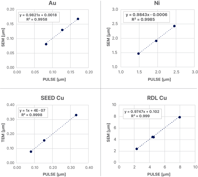
To start with, we conducted a test to confirm the accuracy of picosecond ultrasonic technology when measuring the films typically used in AP: Au, Ni, physical vapor deposition (PVD) seed Cu and RDL Cu (EP). For each film, we used picosecond ultrasonic technology to measure wafers of varying thicknesses. We then cut the wafers for cross-section analysis and estimated the correlation with the picosecond ultrasonic results. Fig. 1. shows the results for the four films. In this scenario, the correlation factor R2 was higher than 0.99 for all four cases, with the slope close to one, clearly demonstrating the accuracy of picosecond ultrasonic measurements.
Following this, we measured product wafers in various interconnect processes with picosecond ultrasonic technology. Fig. 2. shows the process flow for RDL formation.

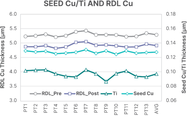
Fig. 3 offers an example of the signal from seed Cu/Ti measured in REF mode and Fig. 4 shows one from RDL in PSD mode. RDL thickness can be measured both in pre- and post-seed Cu removal; 13-point measurement results for seed Cu, Ti and RDL Cu are shown in Figure 5.
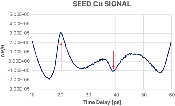
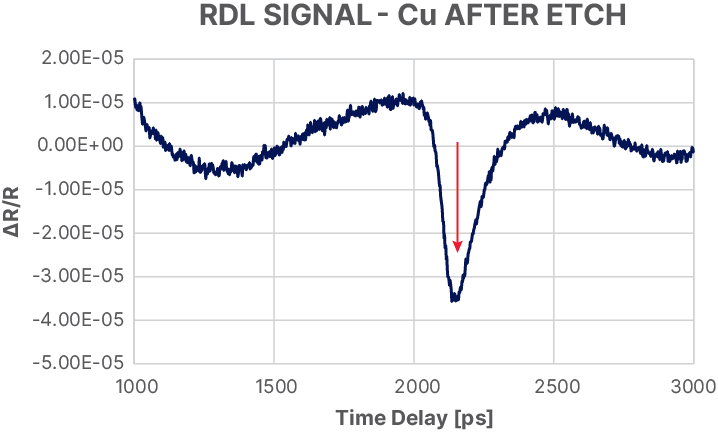
The horizontal axis in the signal figures represents the time delay of the probe pulse with respect to the pump, while the vertical axis represents the change of reflectivity (ΔR/R) caused by the travelling acoustic wave. Time zero is the time when the acoustic wave was generated on the wafer surface. The sharp change of reflectivity in the signal, as demonstrated in Fig. 3 and 4, is mostly due to the acoustic wave reflected from the film interface returning to the surface. In addition, the position of the peak and trough is shown with red arrows. These arrows are directly related to the thickness of the films, seed Cu, barrier Ti and EP Cu. From the position of the peak and trough, the thickness of each film can be calculated.
For seed Cu and barrier Ti, the repeatability of each layer is 0.3% or less of the thickness for all measurements. This demonstrates that picosecond ultrasonic technology is able to meet the necessary 10% gage repeatability and reproducibility requirements. For RDL Cu, the sharp change of reflectivity near 2,200ps corresponds to the round-trip time of the acoustic wave within the RDL Cu film; Cu thickness can be calculated from the trough position. The sharpness of the trough, along with thickness, indicates the trough position can be calculated with good repeatability. In fact, the repeatability of RDL Cu measurements for each point is less than 0.1% of Cu thickness, once again exceeding the 10% gage repeatability and reproducibility requirements.
We also used picosecond ultrasonic technology to measure a bond pad whose film stack is Au/Ni/Cu, with Au being the top film. Fig. 6 shows the schematic of a bond pad with a dimple structure, while Fig. 7 shows an example of an REF mode signal from the bond pad with a dimple structure. Note: this pad is used to bond micro-bumps within a die; the typical pad size is 60μm or larger.
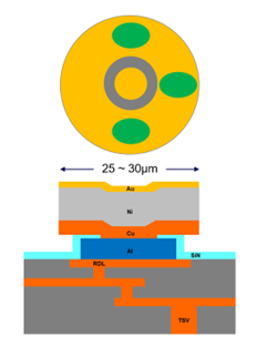
Although the height of the center region of the pad is lower than the surrounding region by a few microns, we could successfully measure individual layer thicknesses by measuring a few sites in the outer ring area and selectively choosing ones with good signal-to-noise ratios. This is possible because the focused spot size of the picosecond ultrasonic beam is 8´10µm2, small enough for the direct measurement on the outer ring of the pad.
Measurement on Interposer Pad with Dimple Structure
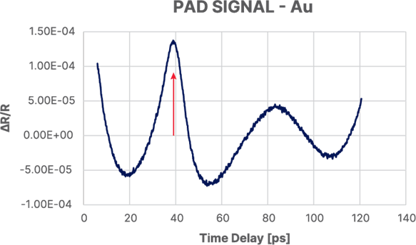
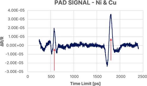
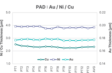
Fig 7: An example of an REF mode signal from the bond pad with a dimple structure for Au (a), Ni and Cu (b), and a 13-point measurement results for Au, Ni and Cu (c).
In Fig. 7a-b, the red arrows indicate the reflectivity changes caused by the acoustic waves returning from the interface to the surface. With these peak positions, we were able to calculate each layer’s thickness with good accuracy and repeatability. The repeatability of Au, Ni and Cu films for each measurement was less than 0.2%, 0.05% and 0.05%, respectively. As such, all three film measurements outperformed the requirement of 10% gage repeatability and reproducibility.
It should be noted that Au film is much thinner than the other two films. As such, there is a significantly higher repeatability for Au films compared with the other films.
Conclusion
Advanced packaging is a highly complex back-end process that involves a variety of technologies. Interconnection technology is one of the most critical parts of packaging because chips are interconnected through metal lines to receive power, exchange signals and, ultimately, operate. Controlling metal thickness and within wafer uniformity in these processes is critical to meeting the requirements for signal integrity in advanced packaging.
In this article, we have demonstrated that picosecond ultrasonic technology can provide a metrology solution with excellent accuracy and gage capability for the control of interconnect processes in advanced packaging. Based on this information, it becomes increasingly clear that picosecond ultrasonic technology is poised to play an increasingly important role in advanced packaging as back-end processes become more like front-end processes.
Acknowledgments
We would like to thank Sanghyun Bae, Junghwan Kim, and Hwanpil Park of Samsung Electronics Co., Ltd., and Kwansoon Park, G. Andrew Antonelli, Robin Mair, Johnny Dai, Manjusha Mehendale and Priya Mukundhan of Onto Innovation for their contributions to this article.
Cheolkyu Kim, Ph.D., is director of product marketing at Onto Innovation with a focus on application development for picosecond ultrasonic (PULSE™) and inspection technologies. Prior to joining Onto, Kim was a postdoctoral research associate in the Physics Department of Brown University. During his three years at Brown, he spent time researching magnetically levitated superfluid liquid helium.
This article was originally posted in the April/May 2025 issue of Semiconductor Digest.
Artificial intelligence is one of the driving forces in today’s semiconductor industry, with more traditional market drivers like high performance compute and smart phones continuing to play important roles. This situation is unlikely change in the years ahead as chip makers continue their quest to create the most advanced nodes. With 3nm nodes in production and 2nm nodes on the horizon, the importance of film measurement only grows in significance as fabs seek to maintain the performance and reliability of cutting-edge devices.
Film metrology is an essential part of semiconductor manufacturing, whether you are dealing with material discovery, technology development, equipment or process control. In a typical semiconductor device manufacturing cycle, there are hundreds of film deposition and removal steps. In addition, film deposition and removal are also commonly used to monitor equipment health. Many of these steps use film measurement tools to ensure that equipment and processes are meeting production requirement.