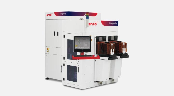
Dragonfly® G3 System
Highly configurable, automated, high speed 2D inspection and 3D metrology for inline process control in advanced packaging, specialty and front-end OQA.


Every day, consumers rely on an invisible network of specialty semiconductor devices without realizing it. The smartphone in your pocket is a good place to start.

May 27 — May 28, 2026
Onto Innovation is a proud exhibitor at IEEE 76th Electronic Components and Technology Conference.
From the cars we drive to the devices we hold and the medical systems that safeguard our health, bipolar-CMOS-DMOS (BCD) technology is at the heart of many modern electronics.
Today’s vehicles are packed with electronics like power engine management, anti-lock braking systems (ABS), airbag controllers, and electric vehicle (EV) charging infrastructure, each one demanding a seamless integration of analog, digital, and power functions. In the case of smartphones, audio amplifiers, and smart home devices, BCD devices help balance power efficiency with high performance. Meanwhile, medical imaging systems, such as ultrasound, and advanced power management solutions, rely on semiconductor technologies like BCD devices to handle diverse electrical requirements without compromising accuracy or safety.
Important as BCD devices may be, what exactly are they?
BCD devices are an advanced semiconductor process technology that integrates three distinct types of transistors—bipolar, CMOS, and DMOS—onto a single chip. The integration of these three transistors enables the simultaneous handling of analog, digital, and power functions within a compact and high-performance platform, with each transistor type contributing unique strengths:
For BCD devices to meet performance expectations, proper process control measures are needed, especially in the case of silicon-chromium (SiCr) thin films.
SiCr films play a critical role in BCD technology, primarily as precision resistive elements within analog and power management circuits (Figure 1.). SiCr resistors offer high stability, low temperature coefficient resistance (TCR), and excellent linearity, making them ideal for applications requiring accurate voltage and current control. Given the stringent reliability standards for BCD technology as demanded by the automotive industry and others, SiCr deposition must exhibit high reproducibility and minimal defectivity to support high-yield manufacturing and robust device performance under thermal and electrical stress.

Figure 1. Schematic of the BCD process, with SiCr film identified.
Uniformity across the wafer and repeatability between lots are critical. After all, minor thickness or compositional variations can lead to resistance drift which impacts analog accuracy and long-term reliability. Tight process control during the deposition step—including chamber stability, target conditioning, and plasma uniformity—ensures consistent film morphology and stoichiometry.
During SiCr sputtering, the precise regulation of specialty gas flow, in particular reactive gases such as nitrogen or oxygen, is critical, as their partial pressures influence plasma chemistry and the kinetics of silicide formation on the substrate. This silicide layer governs nucleation and grain growth, which directly affects grain boundary spacing and, consequently, TCR. Variations in gas flow can alter the stoichiometry and microstructure of the SiCr film, leading to shifts in TCR behavior, including the onset of a pronounced negative coefficient if the process is not tightly controlled.
Given the importance of these demands, manufacturers need the right tools on hand to maintain proper process control and optimize the performances of their BCD devices. In this article we will discuss the application of picosecond ultrasonic technology in two parts: one as a robust thickness metrology solution for qualifying SiCr deposition process and the second for excursion monitoring in BCD devices.
About Picosecond Ultrasonic Technology
Picosecond ultrasonic technology (PULSE™ technology) is a non-contact, non-destructive pump-probe laser acoustic technique for the measurement of metal film thickness. It is a proven workhorse in semiconductor fabs around the world. A 0.1ps laser pulse (pump) is focused to a small (~ 8´10mm2) spot onto a wafer surface to create a sharp acoustic wave. The acoustic wave travels away from the surface through the film at the speed of sound. At the interface with another material, a portion of the acoustic wave is reflected and comes back to the surface while the rest is transmitted. The probe pulse detects this reflected acoustic wave as it reaches the wafer surface. One can detect the change of optical reflectivity that is caused by the strain of the acoustic wave or alternatively detect, using a position sensitive detector (PSD), the deflection of the reflected probe beam that is caused by the deformation of the surface due to the acoustic wave. Both modes, reflectivity (REF) and PSD, are used in characterizing metal films. Knowing the speed of sound in the material, and the arrival time of the echoes, thickness is readily extracted using the first principles technique.
Film Thickness
With background on picosecond ultrasonic technology out of the way, we will turn our attention to the application of this technology as a robust thickness metrology solution for qualifying SiCr deposition process in BCD devices. To demonstrate this, we measured the nominal thickness of SiCr thin films using picosecond ultrasonic technology.
Figure 2a shows the raw data from the SiCr thin film. The acoustic echoes identified in the figure are used to calculate the thickness of the film using the speed of sound and round-trip transit time through the film. Nominally, textbook values for the longitudinal speed of sound would be used. In the case of SiCr films, the longitudinal speed of sound will vary from the bulk material and depend on the deposition process (sputtering, evaporation, etc.) and specific film composition (stoichiometry, density, etc.).
As a one-time calibration, we used cross-section transmission electron microscopy (TEM) to obtain SiCr film thickness and calculated the speed of sound for this specific process to be 69.7Å/ps. The modeled fit to the measurement is shown in Figure 2b.

Figure 2a. Raw data of reflectivity change vs time shown. The cross-wafer variation is identified by the shift in acoustic echoes.

Figure 2b. Modeled fit to measured data shown. The green curve represents the measurement, and the black curve represents the fit.
In Figure 3a, raw data from the DOE skew is shown. The shift in echo position between the different wafers demonstrates the sensitivity of the technique for monitoring the process. Within wafer uniformity profiles from 13 points across the wafer show consistent trends (Figure 3b).
Given the critical function of SiCr films in BCD device architecture, it is imperative to maintain highly uniform deposition with stringent process control to meet electrical and reliability specifications. Yield optimization is directly correlated with film uniformity as variations can significantly degrade device performance and long-term stability. As part of chamber qualification, more extensive sampling across the wafer, including to the edge, was performed (Figure 4). Those profiles are also consistent across the thickness skew.

Figure 3a. Raw data from the DOE thickness skew. Delta represents the skew in thickness from the target. The shift in echo position demonstrates the sensitivity for process monitoring

Figure 3b. Consistent cross wafer uniformity profiles for the three wafers.
Repeatability is a key metric in SiCr thin film metrology for ensuring robust process control and consistent device performance. Poor repeatability can obscure true process shifts, leading to incorrect corrective actions and potential yield loss. Gage capable repeatability measurements ensure compliance with automotive industry standards and are critical for long-term reliability. The dynamic repeatability data indicates performance is better than 0.5Å (1σ) and is more than sufficient to meet the process monitoring needs.

Figure 4. Forty-nine point wafer uniformity profiles for the three wafers, including measurements to the edge of the wafer. The profiles were consistent across the entire wafer.
As demonstrated, picosecond ultrasonic technology provides a precise, non-destructive method for measuring film thickness, validated against TEM calibration. The technique also offers exceptional repeatability and sensitivity, enabling manufacturers to monitor wafer-to-wafer and within-wafer uniformity with confidence. This capability is critical for maintaining tight process windows, as even minor deviations in thickness can lead to resistance drift and compromise analog precision. By integrating this metrology into chamber qualification and process monitoring, fabs can ensure consistent SiCr deposition, optimize yield, and meet stringent reliability standards.
Film quality
In picosecond ultrasonic technology, acoustic echoes are used to calculateSiCr film thickness. However, simultaneously available probe reflectivity data can be leveraged to provide information that can be used for process optimization (i.e., gas flow) and flagging process excursions. As such, this technique can be used to monitor the surface reflectivity of SiCr films; this application serves as a qualitative indicator of the film morphology and surface roughness and can be used for process control.


Figure 5. Surface reflectivity comparison for films having same target thickness but different reflectivity. Average reflectivity variation (top) across wafer is much higher than the thickness variation (bottom). Orange represents the lower flow rate, and blue represents the higher flow rate.
During the sputtering of SiCr films, gas flow has a strong influence on TCR as it impacts the film’s microstructure and stoichiometry (density and composition). This, in turn, determines the film’s stability, stress, and electromigration resistance in BCD applications. Uneven gas distribution causes local variations in thickness and composition leading to resistor mismatches and unpredictable TCR.
The surface reflectivity of the target wafer at two different gas flow rates is shown in Figure 5. Reflectivity data was collected at the same time as the acoustic data and shows the variation in surface reflectivity. At gas flow rate (b), the surface was more reflective corresponding to a smooth, dense film, whereas at flow rate (a), the reduced reflectivity indicates increased surface roughness which can degrade resistor uniformity and TCR stability.
Also, the thickness variation SiCr film is thinner at the higher N2 flow. N2 is known to affect silicide/nitride formation, grain spacing, etc., and impact both thickness and reflectivity. Studies are underway to characterize the impact of annealing temperature. The results are promising.
In summary, the surface quality of SiCr films plays an equally critical role in device stability and long-term performance. The study highlights how reflectivity measurements, captured alongside thickness data using the same picosecond ultrasonic platform, serve as a powerful indicator of film morphology and density. Variations in gas flow during sputtering were shown to significantly influence both reflectivity and thickness, underscoring the importance of precise control over deposition parameters. A smoother, more reflective surface correlates with improved resistor uniformity and predictable TCR behavior, while rougher films can degrade electrical performance.
Based on these results, we have demonstrated that reflectivity measurements, along with thickness measurements, can be leveraged for in-line monitoring to detect deviations in deposition parameters. By leveraging dual metrics—thickness and reflectivity—manufacturers gain a comprehensive, in-line process control solution that enables early detection of excursions and proactive corrections, ensuring robust SiCr thin film integration in advanced BCD architectures.
Conclusion
From automotive safety systems to medical imaging and consumer electronics, BCD technology enables the seamless integration of analog, digital, and power functions that modern applications demand. Yet, this versatility hinges on precise control of SiCr thin films whose stability and uniformity directly influence device reliability
Achieving this level of integration comes with significant manufacturing challenges, particularly in controlling SiCr film thickness and gas flow during sputtering, factors which directly impact resistor stability and temperature performance, which are critical for reliability in demanding environments. To overcome these hurdles, we propose using picosecond ultrasonic technology.
With picosecond ultrasonic technology, manufacturers have a powerful, non-destructive tool for monitoring thickness and reflectivity at the ready, one that ensures that SiCr films meets stringent performance standards. In doing so, manufacturers will be able to safeguard the integrity of BCD devices while supporting the continued evolution of new technologies across the automotive, medical, and consumer electronics sectors.
By Huayuan Li, Alex Hong, Johnny Mu, Timothy Kryman, and Priya Mukundhan
We’d love to connect with you.
Looking to learn more about our innovative solutions and capabilities? Our team of experts is ready to assist you. Reach out today and let’s starts a conversation about how we can help you achieve your goals.
"*" indicates required fields
The Dragonfly G5 system is engineered for inline process control of leading-edge advanced packaging technologies. As the latest generation pattern inspection system in the Dragonfly series, it delivers unparalleled accuracy in detecting submicron defects and performing high-resolution 3D measurements.
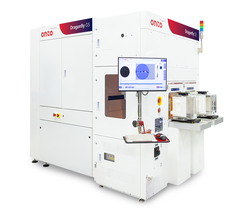
Designed to meet the demands of advanced semiconductor technologies, the Dragonfly G5 system is purpose-built to deliver high-performance, reliable inspection and metrology across complex heterogeneous integration processes. Leveraging next generation high speed line scan 2D imaging and custom-engineered objectives, the system achieves over 3X throughput improvement compared to its predecessor, with submicron sensitivity down to 150nm.
Continuing the legacy of innovation, the Dragonfly G5 system introduces a multi-angle illumination channel that significantly improves signal-to-noise ratio for faint defect detection. Combined with powerful AI-driven algorithms, it enhances both the detectability and classification of critical, yield-impacting defects–empowering fabs to maintain quality and accelerate time-to-yield.
The Dragonfly G5 system expands process control flexibility for wafer-to-wafer and die-to-wafer bonding by integrating high-speed IR imaging to detect sub-surface defects. It incorporates the latest generation of 3Di™ technology, extending bump height metrology capabilities to support next-generation microbumps essential for 3D integration. This enables additional inspection and metrology touchpoints across increasingly complex packaging architectures.




Hybrid bonding enables ultra-dense 3D memory interconnects with up to 1,000x more connections than microbumps. Achieving high yield requires stringent process control, including monitoring topography and detecting particles, cracks and voids. Measuring dishing in copper pads provides valuable insight into surface conditions. Together, these process control insights contribute to improved device reliability and performance.
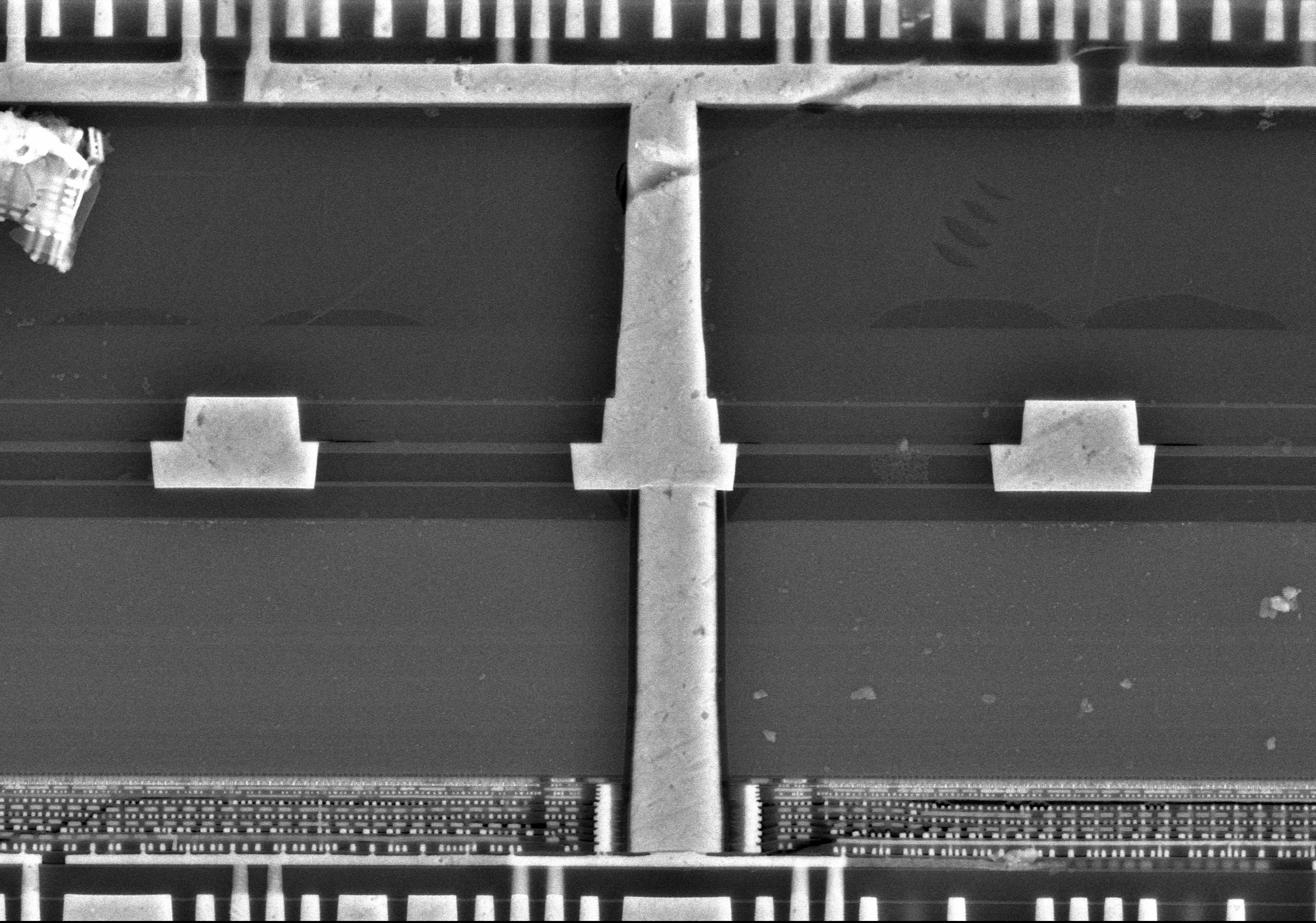
As demand grows for high-performance computing (HPC) and AI-driven applications, manufacturers are turning to hybrid bonding to enable the ultra-dense 3D integration required for next-generation chip architectures. This advanced packaging technology presents significant process challenges. Surface preparation must be precisely controlled to eliminate particles, excess recess, and copper pad dishing, all of which can compromise bond quality. During pre-annealing, particle-induced gaps and wide bonding gaps can prevent proper wafer contact. Post-annealing, the formation of dielectric and metal voids introduces further risks to electrical performance and long-term reliability.
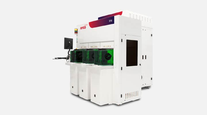
The Iris S system is a versatile platform solution for the advanced packaging and specialty market, supporting 150mm, 200mm and 300mm wafers. It provides thin and thick film, OCD and wafer bow and film stress measurements.
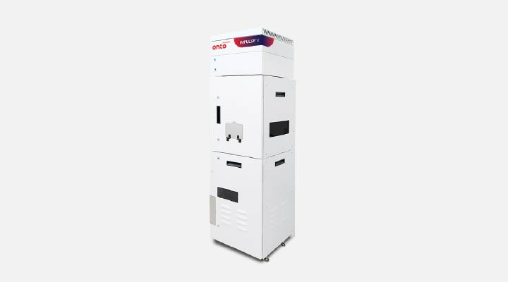
The IMPULSE V system helps to advance CMP processing with enhanced wavefront technology and AI-driven analytics, delivering over 2X precision improvement and faster solutions, crucial for next-gen semiconductor manufacturing demands.
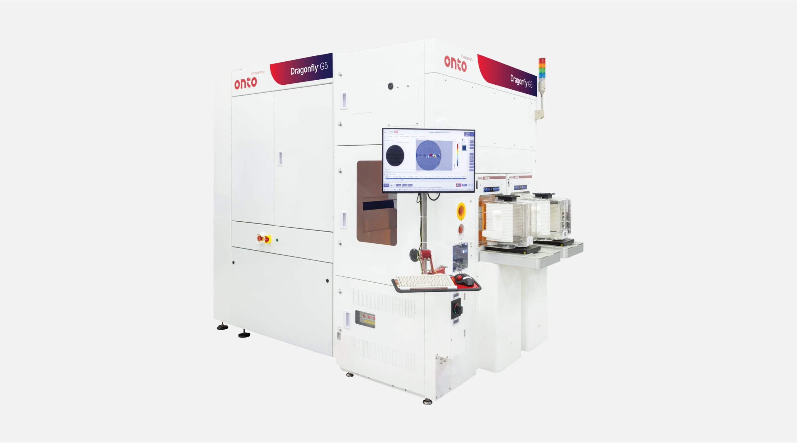
The Dragonfly G5 system is engineered for inline process control of leading-edge advanced packaging technologies. As the latest generation pattern inspection system in the Dragonfly series, it delivers unparalleled accuracy in detecting submicron defects and performing high-resolution 3D measurements.
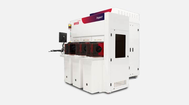
The Aspect System is a revolutionary in-line, non-destructive infrared optical critical dimension (IRCD) system measuring Z-dimension profiling of high aspect ratio structures to enable critical process control. It meets the needs of leading-edge customers with its high speed and process coverage.
As your partner for innovative solutions, we’re always here for you.
Discover how our cutting-edge semiconductor solutions are engineered to meet your most complex challenges: delivering performance, reliability and innovation where it matters most.
"*" indicates required fields
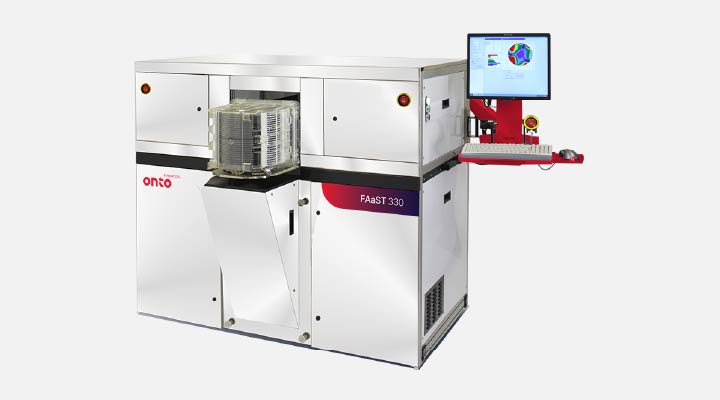
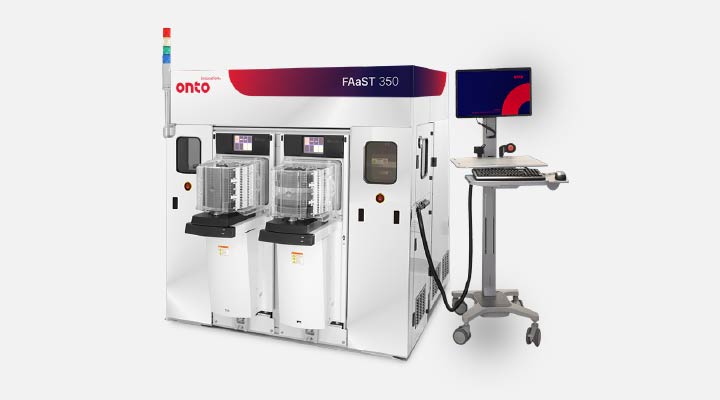
The FAaST system is a versatile, non-contact electrical metrology platform, with an option to combine micro and macro corona-Kelvin technologies together with digital surface photovoltage (SPV). It enables high-resolution dielectric and interface measurements across a wide range of dielectric materials, supporting both R&D and high volume manufacturing.
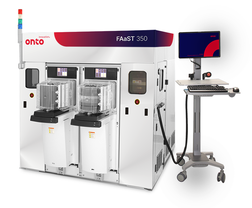
The primary application of non-contact CV metrology is monitoring dielectric properties during IC manufacturing. Unlike conventional electrical measurements, it requires no sample preparation, eliminating the need for MOS capacitor structures. This reduces metrology cost and enables fast data feedback in both R&D and manufacturing environments.
The corona-Kelvin method uses a corona discharge in air to deposit an electric charge (DQC) on the wafer surface. A vibrating Kelvin-probe then measures the resulting surface voltage (V), enabling determination of the differential capacitance (C= DQC/DV). By monitoring surface voltage in both dark and illuminated conditions, the system separates two key components: dielectric voltage (VD) and semiconductor surface potential (VSB), enabling determination of flat band voltage (VFB).
Analysis of the resulting charge-voltage data yields electrical parameters, including trap density (Dit), flat band voltage (Vfb), dielectric charge (Qtot), dielectric capacitance (CD), Equivalent Oxide Thickness (EOT), leakage current, and tunneling characteristics.
As your partner for innovative solutions, we’re always here for you.
Discover how our cutting-edge semiconductor solutions are engineered to meet your most complex challenges: delivering performance, reliability and innovation where it matters most.
"*" indicates required fields
The Aspect S system is a revolutionary in-line, non-destructive model-based infrared reflectometry system that enables critical process control of high aspect ratio structures, films and epitaxial structures. It meets the needs of leading-edge customers with its high speed and process coverage.
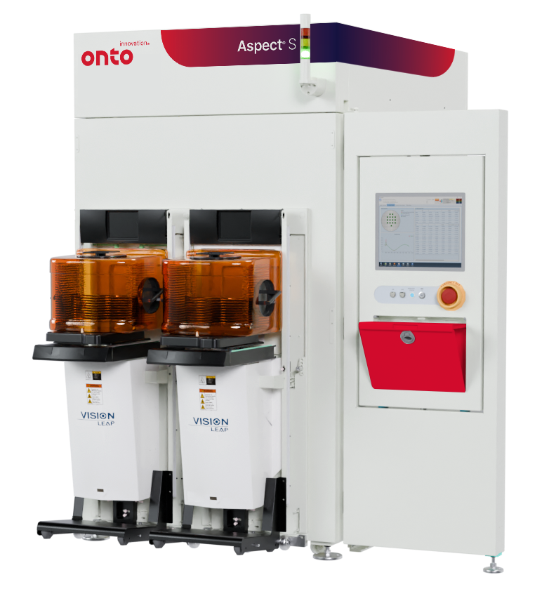
As more high aspect ratio processes are used in multiple industry segments, there are metrology needs for monitoring of related processes, including dimensions and properties of carbon film hard masks and etched 3D structures.
The Aspect S delivers high-throughput, low COO, non-contact, non-destructive measurements of dimensions and uniformity of layers and etched structures used in integrated circuit manufacturing. The small spot size makes the tool suitable for measurements of scribe line test structures as in-line process control. The unique technology and analysis capability simplifies system calibration requirements and removes the effect of substrate variations for key layer measurements.
While the software contains advanced features for measurement recipe and analysis model creation, it has a user-friendly interface and implementation that allows the fab customers to create and manage the recipe system for Aspect S tool fleets.

Thickness map from amorphous carbon film
As your partner for innovative solutions, we’re always here for you.
Discover how our cutting-edge semiconductor solutions are engineered to meet your most complex challenges: delivering performance, reliability and innovation where it matters most.
"*" indicates required fields
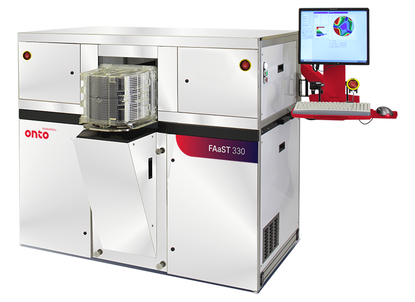
The FAaST Digital SPV system provides a fast, non-contact, and preparation-free method for full wafer imaging of contamination in silicon. High resolution maps of diffusion length and iron (Fe) concentration are generated in minutes, setting the industry standard for precision and sensitivity in Fe contamination control, reaching the E7 cm-3 range.
There is no disputing the detrimental effect of metallic contamination on the integrity of the critical gate oxide used in integrated circuits. During high temperature processing, contamination in the silicon wafer often precipitates at the Si/dielectric interface or segregates into the dielectric—both scenarios can cause premature device failure and reduced yield. As device dimensions shrink, the tolerance for contamination decreases, requiring ever-lower background levels of metals like iron (Fe). Over the past 25 years, the IC industry has reduced typical Fe concentrations by more than three orders of magnitude, yet further reduction is essential, especially for applications like CMOS image sensors.
The FAaST Digital SPV system addresses this challenge with industry-leading sensitivity and speed. It provides a fast, non-contact, and preparation-free method for full-wafer imaging of contamination. High-resolution maps of minority carrier diffusion length and Fe concentration are generated in minutes, enabling fabs to detect and control contamination at levels as low as the E7 cm⁻³ range.

Figure 1. Typical background Fe concentration in new IC Fablines (blue) and the state-of-the-art SPV detection limit (red)
As your partner for innovative solutions, we’re always here for you.
Discover how our cutting-edge semiconductor solutions are engineered to meet your most complex challenges: delivering performance, reliability and innovation where it matters most.
"*" indicates required fields
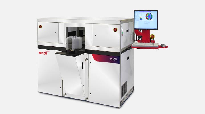
The CnCV system enables wafer-level characterization of WBG materials without test device fabrication, reducing time and cost. As a mercury-free alternative to MCV, it eliminates contamination concerns. The enhanced Kinetic CV mode with UV-assisted corona charge neutralization achieves high throughput and precision for fast, reliable process control.
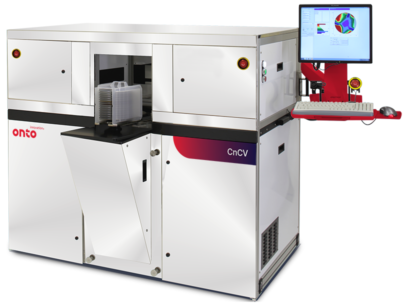
The CnCV system utilizes a novel constant surface potential corona charging, which enables the precision required over a large voltage range. The patented technology includes charge- and photo-assisted modes, especially suited for speed and precision on WBG materials and structures, including SiC, Ga2O3, GaN, and AlGaN/GaN HEMT. Additionally, Corona-Kelvin characterization includes electrical properties of dielectrics and interfaces of films on SiC and GaN epi layers. An automated top-side edge contact (TSEC) is also available enabling characterization of WBG on insulating/semi-insulating substrates. Automated bias-temperature stress (BTS) measurements are also available with the CnCV system, providing a fast, noncontact way to quantify the reliability of passivated SiC and GaN.
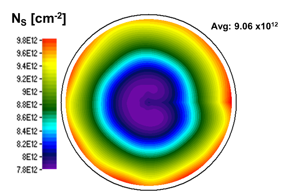
Beyond typical CV type parameters, the full wafer corona approach allows for QUAD (quality, uniformity, and defect) mapping. The electrical defect imaging, QUAD-EDI, mode is especially designed for SiC. It provides a unique means for quick screening of epi electrical defectivity enabling improvement in device yield prediction.

Figure 1. QUAD-EDI Map on final metallized device wafer after Merged Schottky PiN diode fabrication identifying failed dies.
As your partner for innovative solutions, we’re always here for you.
Discover how our cutting-edge semiconductor solutions are engineered to meet your most complex challenges: delivering performance, reliability and innovation where it matters most.
"*" indicates required fields