
Discover® Run-to-Run Software
Automating process control with precision and efficiency

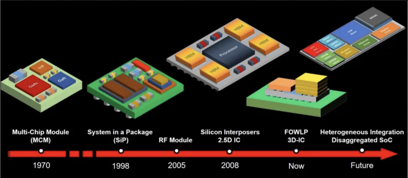
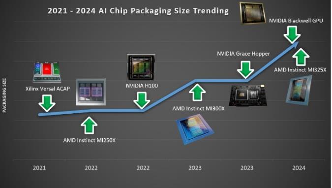
If you’ve been following the evolution of advanced packaging, you know that the industry is pushing boundaries like never before. From high-performance computing to industry-upending AI devices, the demand for smaller, faster, and more powerful chips is driving innovation at every level.

Discover RMS software is a complete solution for recipe management. This unified repository automatically delivers the right recipe to the right system at the right time.
Discover RMS software is a factory-level recipe management system that provides a central server repository for all recipes. This system allows desktop access for editing and includes complete version control of all recipes used within the fab.
When coupled with Discover Run-to-Run software, it fundamentally tracks all control changes by automatically inserting recipe values into the recipe body. Working in concert with your MES system, recipes are automatically selected and downloaded to the right tool to be executed on the right material. The recipe sign-off feature enforces a tight control of recipes by ensuring customer approval of any large changes.
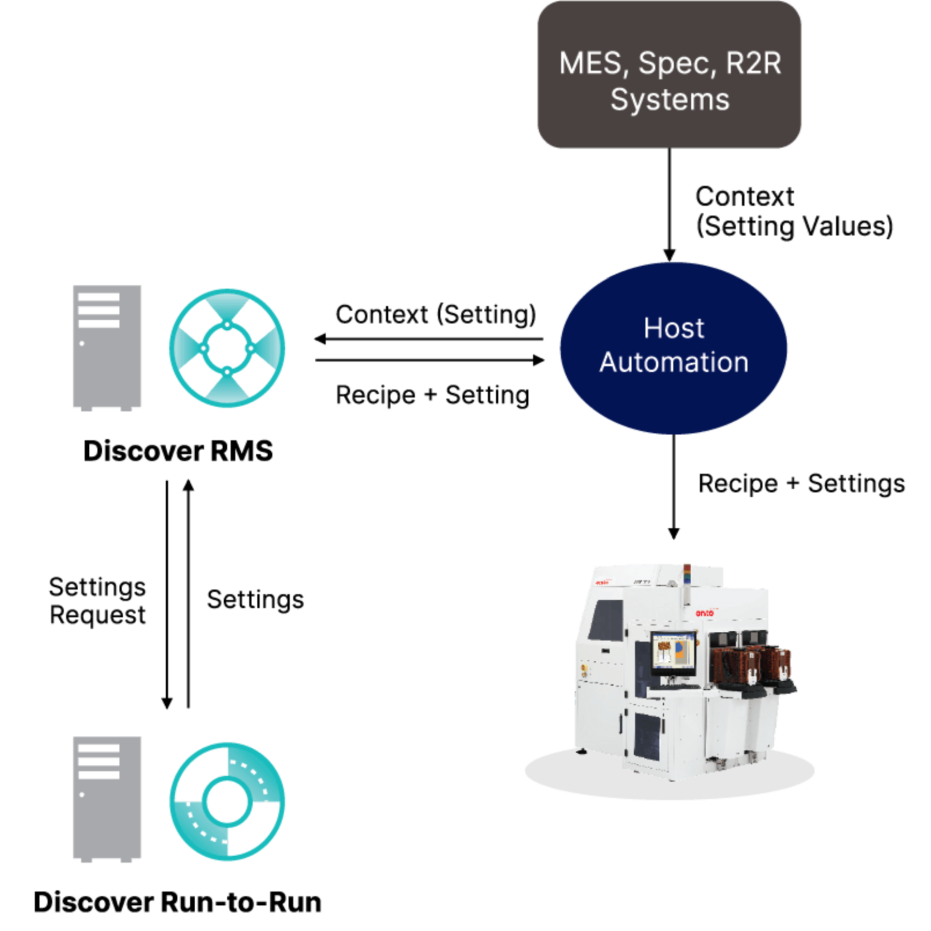
The Discover RMS Process

As your partner for innovative solutions, we’re always here for you.
Discover how our cutting-edge semiconductor solutions are engineered to meet your most complex challenges: delivering performance, reliability and innovation where it matters most.
"*" indicates required fields
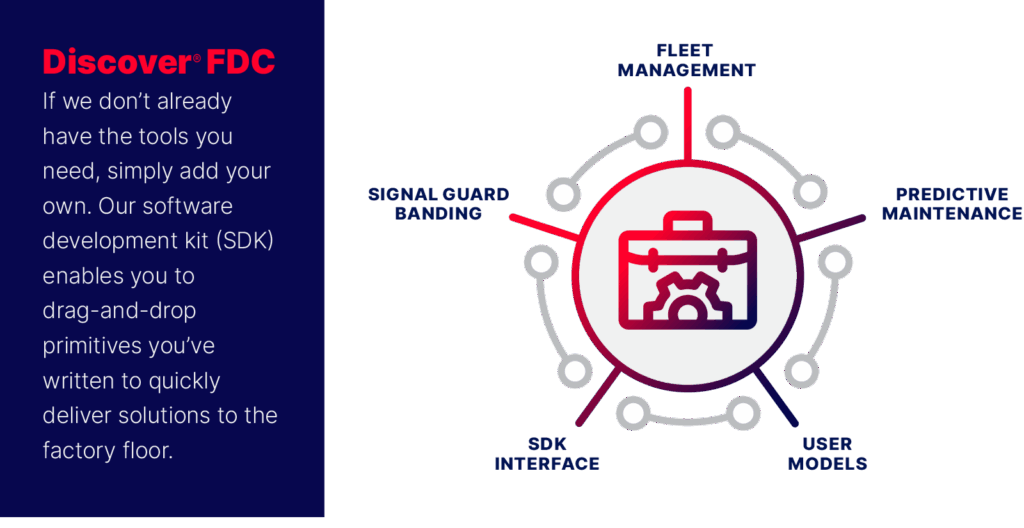
Discover FDC software is part of a robust data management suite, serving as the ideal gateway to digital transformation and unlocking Industry 4.0 best practices for impactful results.
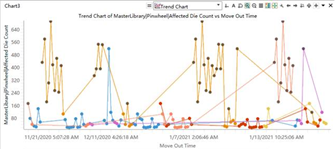
Discover FDC software transforms tool sensor data into actionable insights. It empowers manufacturers to optimize fab efficiency, scaling seamlessly to high-volume manufacturing while reducing tool downtime by detecting anomalies early. With its diverse set of flexible controls and real-time data analysis, Discover FDC software enhances productivity, improves cycle time and increases equipment availability (OEE). Its user-friendly interface integrates advanced process control, allowing engineers to pinpoint issues and bring equipment online faster. Proven across processes and operational modules, it eliminates wasted time and energy by preventing idle tools and minimizing scrapped wafers. When connected to Discover Defect and Discover Yield software, Discover FDC software identifies meaningful correlations that drive even greater efficiency and production results. This robust solution redefines control, setting a new standard for achieving maximum enterprise-wide factory performance. That’s control, redefined.


As your partner for innovative solutions, we’re always here for you.
Discover how our cutting-edge semiconductor solutions are engineered to meet your most complex challenges: delivering performance, reliability and innovation where it matters most.
"*" indicates required fields
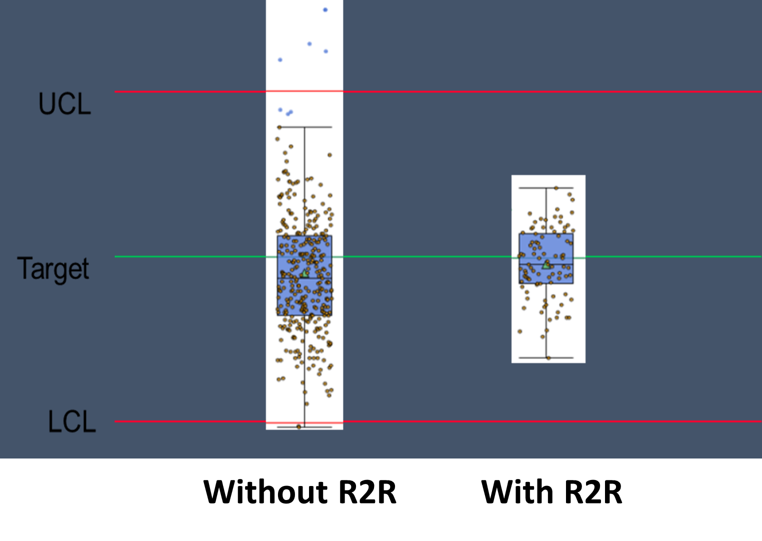
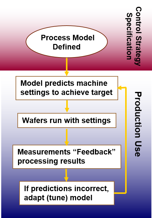
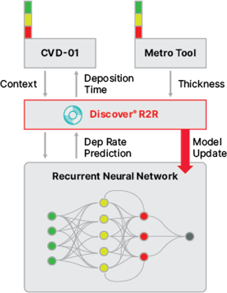
Discover Run-to-Run software boosts profits and productivity with swift deployment on any process or tool, increasing Cpk and throughput while reducing pilot wafers, engineering time and manufacturing costs.
Discover Run-to-Run software is a feature-rich application that enables advanced supervisory process control, surpassing traditional statistical methods. It ensures precise process goals. For example, achieving desired thickness is possible through tailored adjustments of machine parameters like deposition duration or pressure settings. Designed for high-mix production, it allows seamless transfer of control strategies across factories for operational flexibility. Proven globally, it operates thousands of tools across hundreds of processes continuously. With its adaptable, framework-based APC solution, Discover Run-to-Run software enables rapid factory-wide deployment, delivering significant and immediate return on investment while enhancing consistency, productivity and efficiency.


As your partner for innovative solutions, we’re always here for you.
Discover how our cutting-edge semiconductor solutions are engineered to meet your most complex challenges: delivering performance, reliability and innovation where it matters most.
"*" indicates required fields
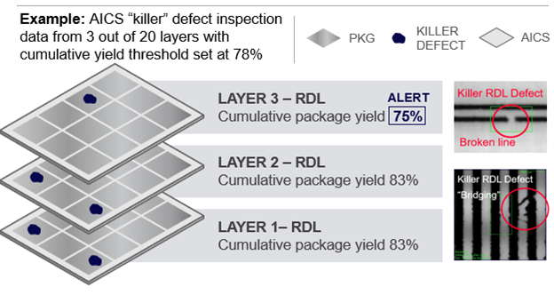
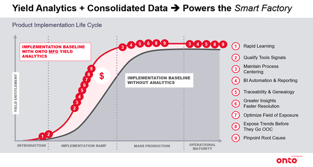
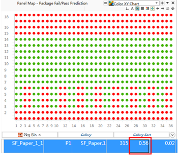
Discover Yield software is a complete yield management enterprise platform that combines parametric, defect and yield optimization with data mining and workflow development across all data sources from memory and design to assembly and packaging.
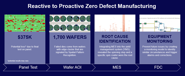
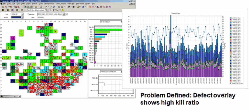
Discover Yield software helps reduce the time it takes to find root causes of yield excursions and enables manufacturers to broaden their analysis scope for better yield management.
The software includes data acquisition and integration, a development environment through workflow and scripting, and specialized analysis algorithms to identify domain-specific issues, such as data mining, spatial anomalies, wafer processing sequence problems, commonality of effects, system and random yield loss, chamber matching, tool events, traceability and more. In addition, Discover Yield software provides distinct tools – principal components and multivariate analysis of variance (MANOVA) – that allow systematic, simultaneous examination of multiple variables. Discover Yield software’s database architecture for genealogy uniquely supports value chain predictive analytics.
Improving baseline yield with analytics


As your partner for innovative solutions, we’re always here for you.
Discover how our cutting-edge semiconductor solutions are engineered to meet your most complex challenges: delivering performance, reliability and innovation where it matters most.
"*" indicates required fields
An advanced feed-forward lithography software solution for fan-out panel level packaging that enhances yield and throughput by correcting die placement errors through external measurements, predictive analytics and adaptive shot control.
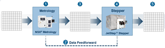
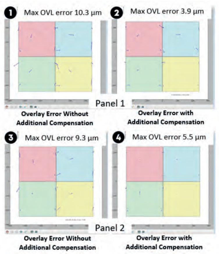
StepFAST® software is Onto Innovation’s advanced lithography software solution tailored for fan-out panel-level packaging, where die placement errors and material instability can significantly impact yield and productivity. StepFAST® software uses a feed-forward adaptive shot approach, integrating high-speed die placement measurements from the Firefly® system and applying real-time corrections to every shot of the JetStep® lithography tool. This external measurement strategy doubles throughput compared to traditional on-tool (self-metrology) methods. The software also incorporates predictive yield analysis, enabling dynamic adjustment of exposure field sizes to balance throughput and overlay accuracy. By automating reticle selection and optimizing field coverage, StepFAST® software ensures efficient panel exposure while minimizing registration errors—from ±50µm down to under ±3µm. With advanced analytics, StepFAST® software transforms lithography into a flexible, high-efficiency process, delivering substantial improvements in yield, throughput, and cost of ownership for panel-level packaging applications.
Die shift on reconstituted panels can significantly impact both productivity and yield. To address this challenge, we use a parallel die placement measurement process and advanced analytics to provide a means to balance productivity against yield. Our integrated lithography cell, featuring Firefly inspection, StepFAST software, and JetStep Lithography, delivers industry-leading throughput and yield for fan-out panel level packaging.
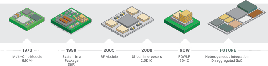
It is well understood that advanced packaging applications require high performance, low cost, increased functionality and improved reliability that 2.5D and 3D packaging solutions provide. Fan-out panel-level packaging (FOPLP) is one of the technologies that has the potential to meet these packaging requirements.
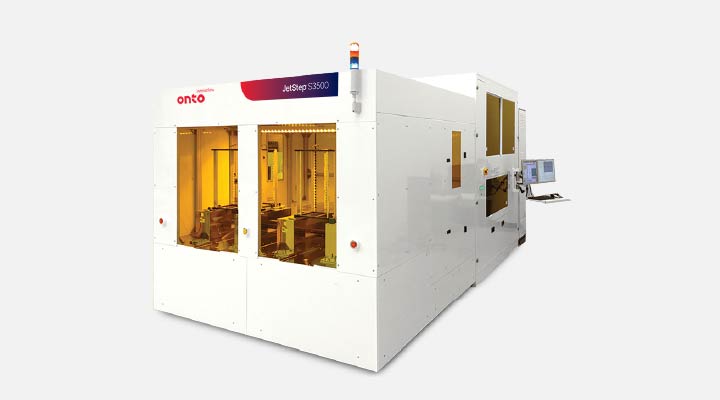
The JetStep S3500 system is designed to provide OSATS with a high-volume manufacturing advanced packaging lithography solution. For substrates up to 720mm x 600mm, it supports fan-out panel level packaging.
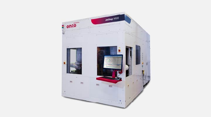
The JetStep X500 system is designed to provide AICS and OSAT manufacturers with a high-volume manufacturing lithography solution for heterogeneous integration. The JetStep X500 system exposes panel-type substrates made of CCL, FR4, composite, glass or other materials.
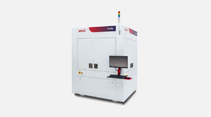
The Firefly G3 system provides automated inspection and 3D metrology for advanced IC substrates and panel level packaging, delivering high resolution and productivity for demanding applications like high-performance computing (HPC), artificial intelligence (AI), cloud computing and machine/deep learning.

An advanced feed-forward lithography software solution for fan-out panel level packaging that enhances yield and throughput by correcting die placement errors through external measurements, predictive analytics and adaptive shot control.
As your partner for innovative solutions, we’re always here for you.
Discover how our cutting-edge semiconductor solutions are engineered to meet your most complex challenges: delivering performance, reliability and innovation where it matters most.
"*" indicates required fields
The JetStep X500 system is designed to provide AICS and OSAT manufacturers with a high-volume manufacturing lithography solution for heterogeneous integration. The JetStep X500 system exposes panel-type substrates made of CCL, FR4, composite, glass or other materials.
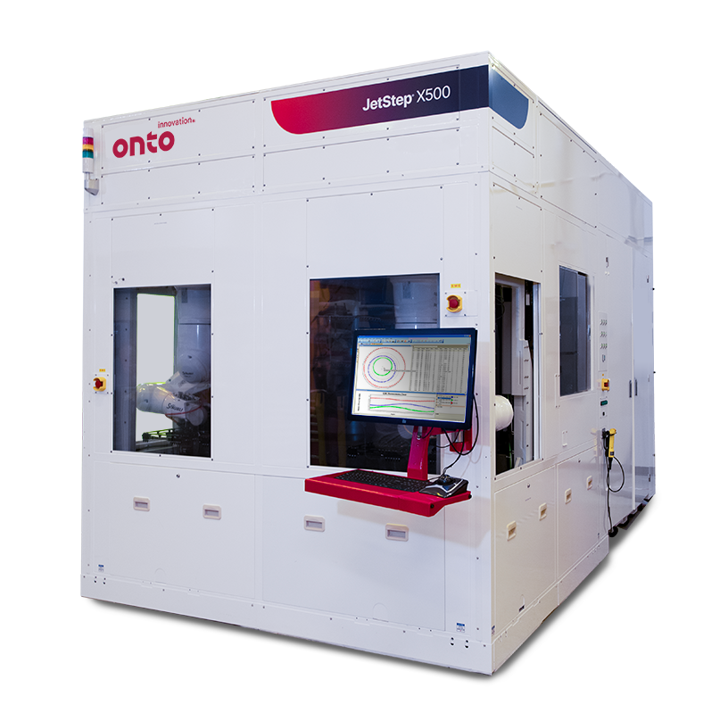
The JetStep X500 panel lithography system is optimized for high volume manufacturing of high-end AICS and other advanced packaging panel applications. As we approach the limits of Moore’s law, the JetStep X500 system addresses the need for extremely large packages integrating multi-node chips, or “chiplets,” enhancing functionality, speed, I/O count and reducing power consumption for server farms, AI, and mobile applications. The JetStep X500 system features the industry’s largest exposure field , fine line RDL resolution with large depth of focus (DOF), excellent overlay accuracy, and automatic magnification compensation with independent x and y magnification adjustment. The JetStep X500 system handles a large range of substrate thicknesses with high levels of warp, offering unique imaging parameter control to compensate for panel distortion. Additionally, it can run highly warped substrates with an edge clamping option and provides real-time autofocus at every exposure site to compensate for challenging topography.


Die shift on reconstituted panels can significantly impact both productivity and yield. To address this challenge, we use a parallel die placement measurement process and advanced analytics to provide a means to balance productivity against yield. Our integrated lithography cell, featuring Firefly inspection, StepFAST software, and JetStep Lithography, delivers industry-leading throughput and yield for fan-out panel level packaging.
It is well understood that advanced packaging applications require high performance, low cost, increased functionality and improved reliability that 2.5D and 3D packaging solutions provide. Fan-out panel-level packaging (FOPLP) is one of the technologies that has the potential to meet these packaging requirements.
The JetStep S3500 system is designed to provide OSATS with a high-volume manufacturing advanced packaging lithography solution. For substrates up to 720mm x 600mm, it supports fan-out panel level packaging.
The JetStep X500 system is designed to provide AICS and OSAT manufacturers with a high-volume manufacturing lithography solution for heterogeneous integration. The JetStep X500 system exposes panel-type substrates made of CCL, FR4, composite, glass or other materials.
The Firefly G3 system provides automated inspection and 3D metrology for advanced IC substrates and panel level packaging, delivering high resolution and productivity for demanding applications like high-performance computing (HPC), artificial intelligence (AI), cloud computing and machine/deep learning.
An advanced feed-forward lithography software solution for fan-out panel level packaging that enhances yield and throughput by correcting die placement errors through external measurements, predictive analytics and adaptive shot control.
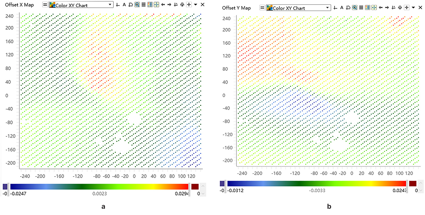
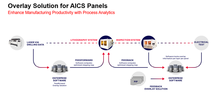
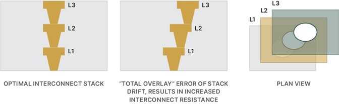
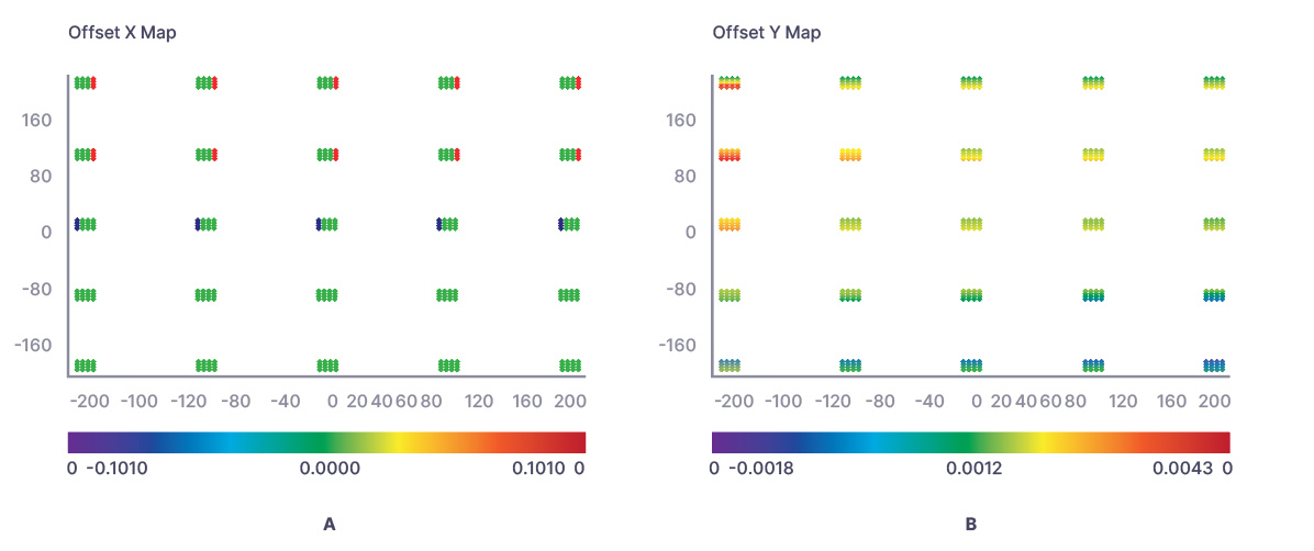
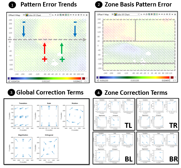
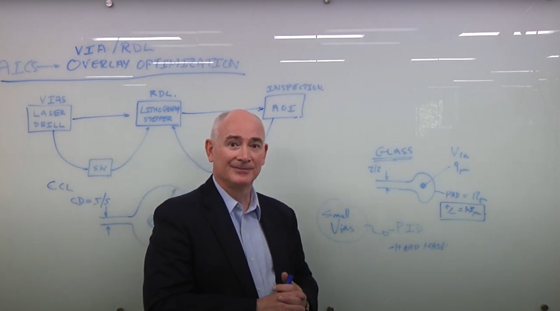
During the processing of organic (CCL) advanced IC substrates (AICS) the substrates become distorted which impacts the overlay of Via to RDL pad structures. To solve this problem, the stepper must adjust the alignment solution to match the previous layer’s distortion by measuring the overlay. Proprietary software provides the user with the ability to adjust each zone of the AICS with independent offsets.
The growing demand for heterogeneous integration is driven by the 5G market. This includes smartphones, data centers, servers, high-performance computing (HPC), artificial intelligence (AI) and internet of things (IoT) applications. Next generation packaging technologies require tighter overlay to accommodate larger package sizes with fine-pitch chip interconnects on large-format flexible panels.
Designed for advanced IC substrates (AICS), it incorporates a large field exposure area with a large depth of focus. Proprietary software enables independent zone offset adjustments across the AICS.
The Firefly G3 system provides automated inspection and 3D metrology for advanced IC substrates and panel level packaging, delivering high resolution and productivity for demanding applications like high-performance computing (HPC), artificial intelligence (AI), cloud computing and machine/deep learning.


As your partner for innovative solutions, we’re always here for you.
Discover how our cutting-edge semiconductor solutions are engineered to meet your most complex challenges: delivering performance, reliability and innovation where it matters most.
"*" indicates required fields