
Dragonfly® G5 System
The latest generation inline pattern inspection system in the Dragonfly series, delivering sub-micron defect detection and high resolution 3D metrology.

If you’ve been following the evolution of advanced packaging, you know that the industry is pushing boundaries like never before. From high-performance computing to industry-upending AI devices, the demand for smaller, faster, and more powerful chips is driving innovation at every level.

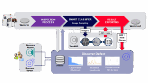
The native integration of the Discover software platform boosts tool throughput and enhances inspection quality by capturing more defects of interest. It provides a complete reduced review solution utilizing advanced machine learning (ML) and artificial intelligence (AI) technologies, customized to meet unique customer needs.
Optimized Image Capture for Inspection Tools
Discover software enhances inspection quality and tool throughput by optimizing the image capture sample plan.
AI-Powered Automatic Defect Classification (TrueADC Software)
Integrated AI-based classification improves device quality and yield, driving fab efficiency and productivity.
Streamlined Review Software
Reduced review best practices improve operator productivity, enhance engineering review quality, and shorten review time.
Advanced Defect Analytics
Comprehensive inline wafer/panel monitoring enables automatic alarm notifications, detailed reports and Out-of-Control Action Plans (OCAPs).
Defect Source Analysis
Enables actionable process feedback to improve manufacturing outcomes.
Automated Business Analysis with Report Server
Boosts engineering productivity by up to 25% and supports multiple production report formats.
Machine Learning-Based Pattern Detection
The Discover Patterns software module proactively identifies wafer-level systematic yield-limiting issues and classifies them for analytics, enabling both process feedback and feedforward.
Centralized Defect & Metrology Management
Built on a scalable Big Data and high-availability architecture, this solution supports advanced applications such as high volume manufacturing (HVM) bump metrology, capable of handling wafers with over 100 million bumps.


As your partner for innovative solutions, we’re always here for you.
Discover how our cutting-edge semiconductor solutions are engineered to meet your most complex challenges: delivering performance, reliability and innovation where it matters most.
"*" indicates required fields
A suite of OCD modeling software and computing hardware that enables the full capability and connectivity across all Onto OCD and thin film metrology systems, including Atlas, Aspect, Iris and IMPULSE systems.
Onto Innovation’s OCD technology offers powerful modeling and computing packages to support various phases of film and OCD measurement setup, data management, and fleet management. These capabilities include model building, runtime data analysis, system calibration, data analytics, data connectivity and management, spectrum management and fleet matching.
Onto OCD solutions consist of several modeling and computing components, including Ai Diffract™ modeling software, runtime onboard computer, offline modeler, offline model building clusters, and recipe & data management server. Each component seamlessly extends OCD capabilities to Onto’s standalone and integrated metrology systems, providing end-to-end capabilities from offline recipe support and development to fab-wide networking and connectivity for easy fleet management.
Ai Diffract software is a powerful modeling, visualization and analysis software with an intuitive 3D modeling interface to simplify the building and visualization of today’s most complex semiconductor devices. It offers OCD modeling and advanced machine learning capabilities, next-generation real-time regression, offline sensitivity analysis tools and comprehensive GUI and structure input for true multi-variant modeling. Ai Diffract software’s proprietary fitting algorithms enable fast and accurate calculations for signal processing, helping ensure high fidelity model-based measurements. Automation features for spectral fitting, recipe optimization, and sensitivity analysis offer great user productivity. The first-in-market AI-guided engine synergizes physics-based modeling and machine learning to deliver the most robust solution with quick time to solution.
Ai Diffract Modeler is the offline analytical engine that allows users to create and edit recipes offline. It supports multiple users and can connect to Ai Diffract cluster for high intensity computing.
Ai Diffract Onboard is the on-tool runtime engine that maximizes tool throughput for complex use cases. It ensures rapid analysis without interfering with system operation or impacting throughput.
Ai Diffract Cluster is an enterprise scale computing server deployed for offline recipe development or in-line real-time regression. Optimized to support the workload of Ai Diffract software analysis, it scales based on fleet size, recipe numbers, and computing intensity.
Recipe Distribution Server (RDS) / Nexus Servers is a fab-wide networking and server system for fleet management and connectivity. RDS/Nexus servers provide connectivity and support to Ai Diffract recipe management and distribution, data/spectrum feed-forward and feedback, spectrum management, and fleet management.


As your partner for innovative solutions, we’re always here for you.
Discover how our cutting-edge semiconductor solutions are engineered to meet your most complex challenges: delivering performance, reliability and innovation where it matters most.
"*" indicates required fields
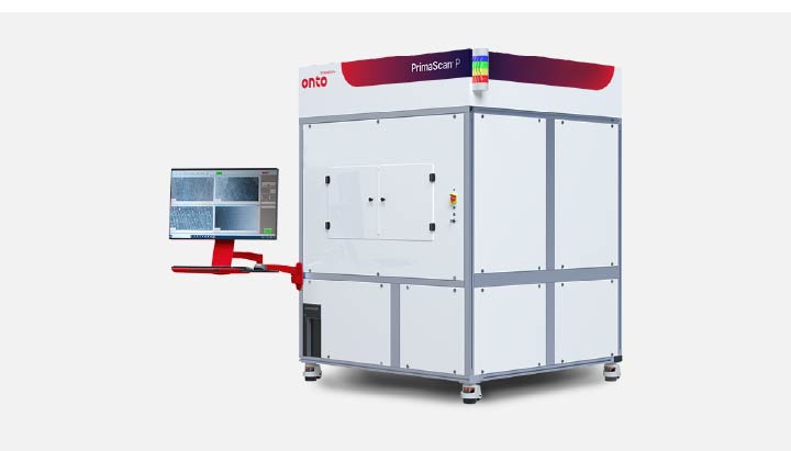
The PrimaScan wafer defect inspection system delivers a flexible, high sensitivity solution at the lowest cost of ownership per pass.
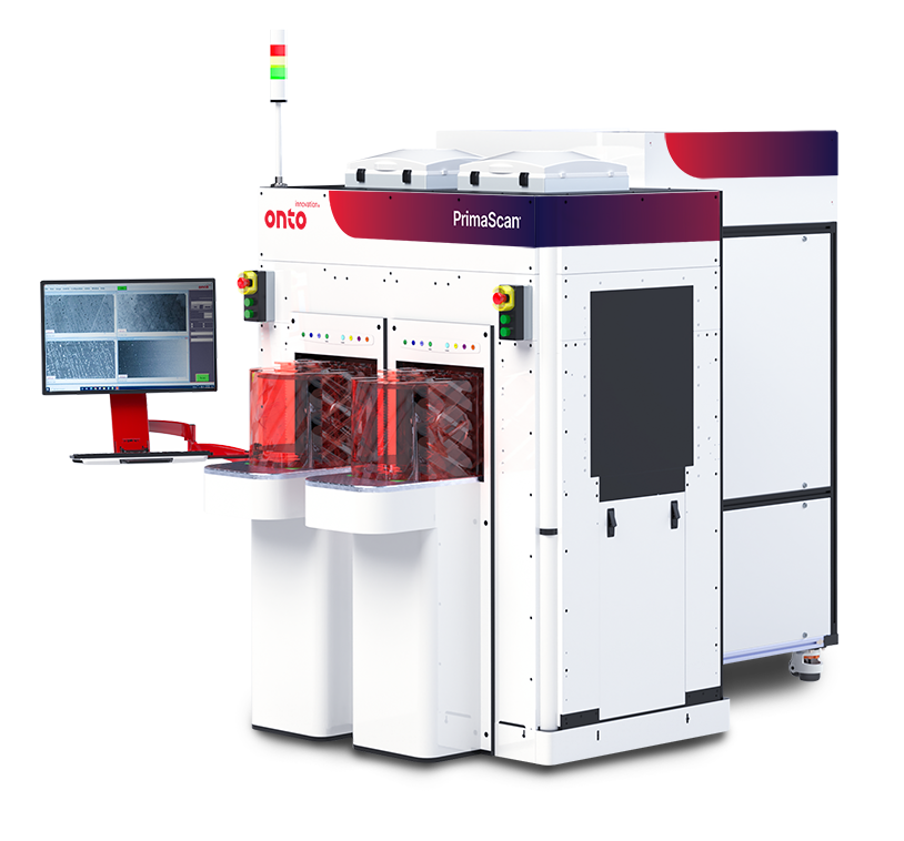
The PrimaScan system utilizes laser scatterometry and imaging techniques leveraging proprietary optics and sensing technologies for reliable inspection of nanometer sized defects on a variety of opaque and transparent/semi-transparent substrates suitable for either R&D or high-volume manufacturing environments. With multiple detection channels, the system can detect, measure, characterize and image surface particles, scratches, pits, bumps, surface contamination, film or bulk wafer stress, voids/inclusions, including chips and cracks at the wafer edge.
The PrimaScan system addresses challenges in both incoming wafer quality control and in inline process monitoring. Capable of handling multiple substrate materials, it uniquely addresses inline process defect and contamination monitoring in wafer-based production environments.
Designed with versatility in mind the PrimaScan system can handle a variety of wafer sizes and substrate types

As your partner for innovative solutions, we’re always here for you.
Discover how our cutting-edge semiconductor solutions are engineered to meet your most complex challenges: delivering performance, reliability and innovation where it matters most.
"*" indicates required fields
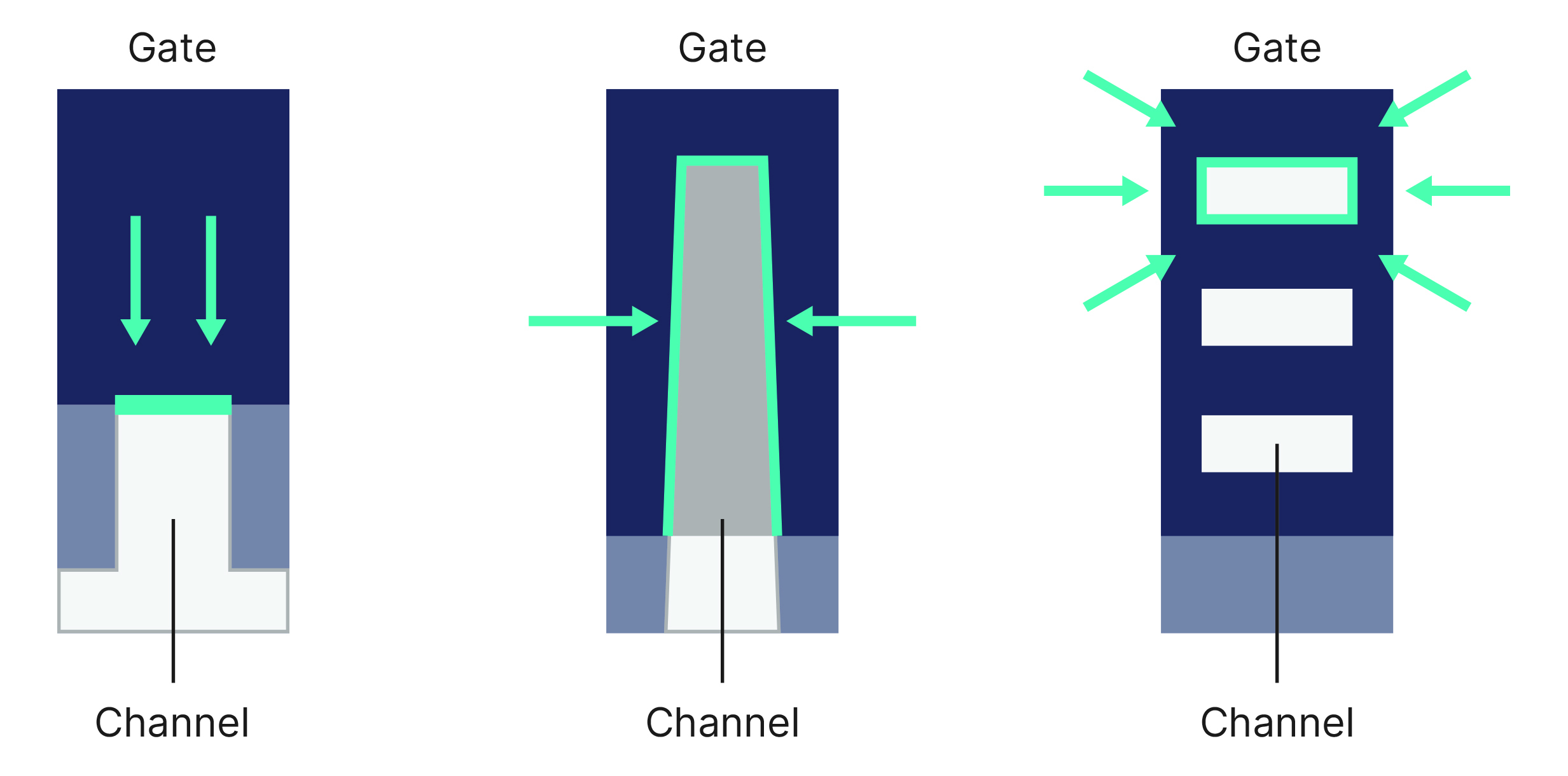
Heterogeneous integration is a key enabler of today’s AI innovations. By bringing together multiple chips with different functionalities, a.k.a., chiplets, AI devices have been able to achieve tremendous performance gains. However, the heterogeneous integration of advanced packages has its own set of process control obstacles that must be addressed, including new interconnect challenges involving redistribution layers (RDL) and bond pads.
Recently, Onto Innovation and Samsung Electronics Co., Ltd., teamed up to explore how picosecond ultrasonic technology could be used to measure the metal thickness of RDL and bond pads in high performance AI packages. In this blog, the second in our series on the advanced packaging applications of picosecond ultrasonic technology, we will show how this technology can be used to measure metal films during RDL and bond pad processes.
But first, a word about picosecond ultrasonic technology, a widely adopted non-contact, non-destructive acoustic technique that can be used to measure film thickness.
Measuring Films
Picosecond ultrasonic technology measures film thickness by tracking the round-trip travel time of ultrasonic waves generated and detected using an ultrafast laser pump probe technique. A short laser pulse (pump) creates an acoustic wave that travels through the film, reflects at material interfaces, and returns to the surface. A second laser pulse (probe) detects the returning wave.
Two detection methods can be used to determine film thickness or properties:
By measuring the time it takes for the wave to return and knowing the speed of sound in the material, the film thickness can be accurately determined to sub-angstrom levels.
This level of layer-specific metrology, precision, and measurement repeatability is increasingly critical as AI-driven packaging pushes the limits of interconnect density and uniformity.
Accuracy and Repeatability
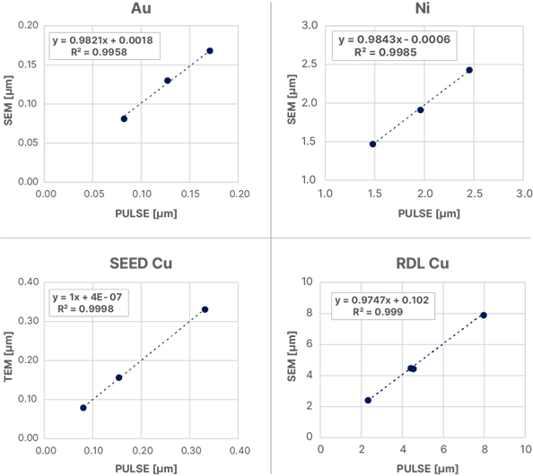
For the purpose of our exploration, we conducted a test to confirm the accuracy of picosecond ultrasonic technology when measuring the films typically used in advanced packaging. These metals include Au, Ni, physical vapor deposition (PVD) seed Cu, and RDL Cu (EP). For each film we used picosecond ultrasonic technology to measure wafers of varying thicknesses. Then we cut the wafers for cross-section analysis and estimated the correlation with the picosecond ultrasonic results for the four films (Figure 1). In this scenario, the correlation factor R2 was higher than 0.99 for all four cases, with the slope close to one, demonstrating the accuracy of picosecond ultrasonic measurements.
This level of correlation is not only impressive, it is essential. Competing technologies such as four-point probe (4PP) or contact profilometry often fall short in multilayer structures or non-planar surfaces, where mechanical contact can distort results or damage delicate features.
Following this, we measured product wafers in various interconnect processes with picosecond ultrasonic technology, including seed Cu/Ti measured in REF mode (Figure 2) and RDL in PSD mode (Figure 3). RDL thickness can be measured both in pre- and post-seed Cu removal.
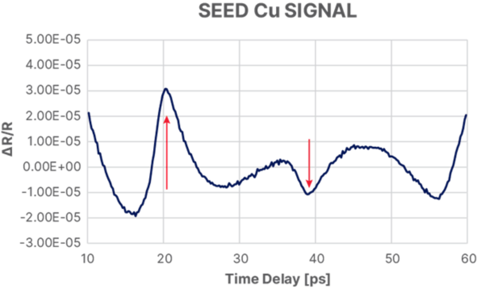
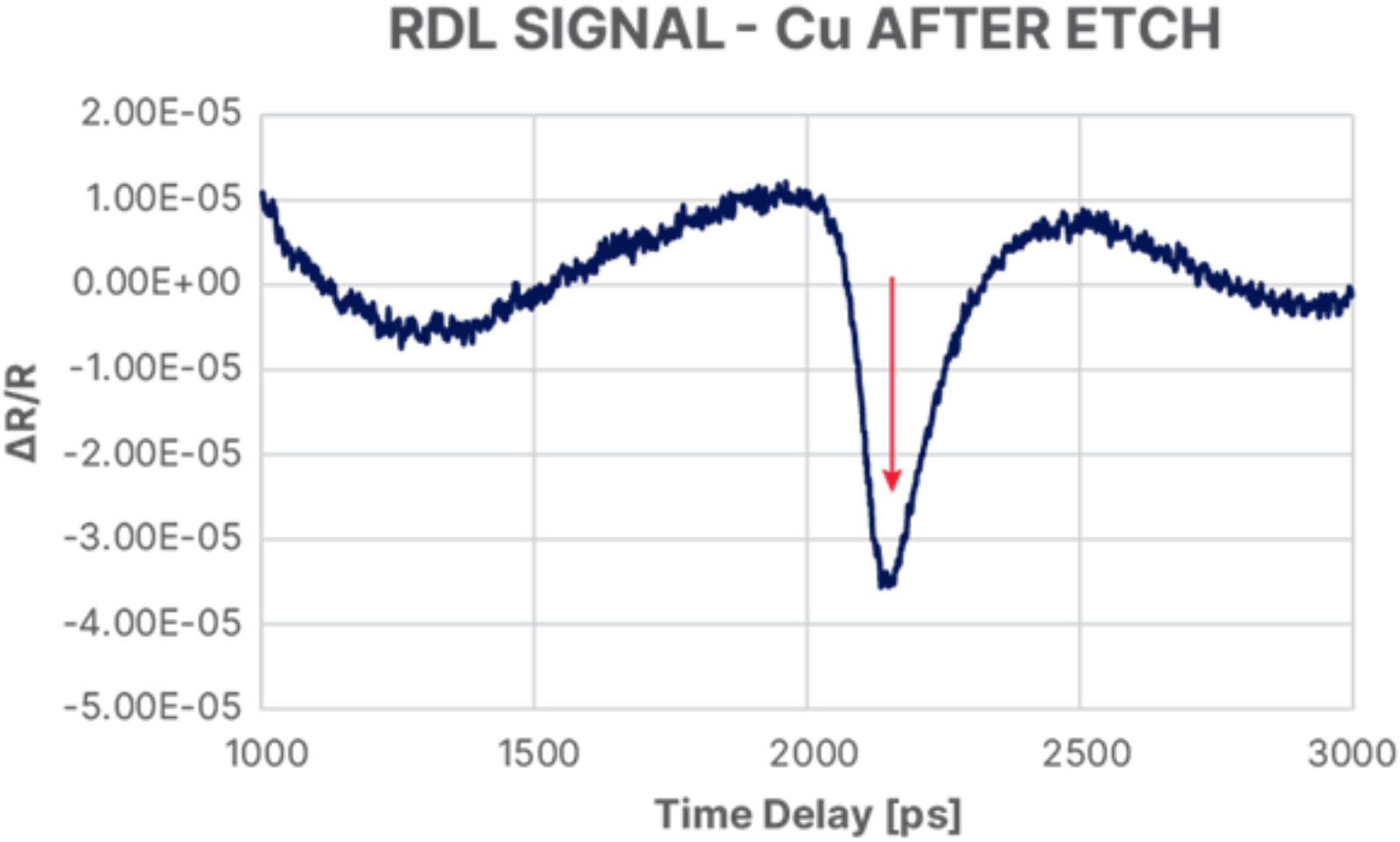
The horizontal axis in Figures 2 and 3 represents the time delay of the probe pulse with respect to the pump, while the vertical axis represents the change of reflectivity (ΔR/R) caused by the travelling acoustic wave. The sharp change of reflectivity in the signal, as demonstrated in Figures 2 and 3, is mostly due to the acoustic wave reflected from the film interface returning to the surface. In addition, the position of the peak and trough is shown with red arrows. These arrows are directly related to the thickness of the films, seed Cu, barrier Ti, and EP Cu. From the position of the peak and trough, the thickness of each film can be calculated. For seed Cu and barrier Ti, the repeatability of each layer is 0.3% or less of the thickness for all measurements. This demonstrates the capability of picosecond ultrasonic technology to meet 10% gage repeatability and reproducibility requirements.
For RDL Cu, the sharp change of reflectivity near 2,200 picoseconds (ps) corresponds to the round-trip time of the acoustic wave within the RDL Cu film; Cu thickness can be calculated from the trough position. The sharpness of the trough, along with thickness, indicates the trough position can be calculated with good repeatability. In fact, the repeatability of RDL Cu measurements for each point is less than 0.1% of Cu thickness, once again exceeding the 10% gage repeatability and reproducibility requirements.
Such precision is a necessary technical achievement. As AI applications demand tighter control over signal integrity and power efficiency, the margin for error in interconnect thickness shrinks dramatically. Legacy tools simply cannot keep up.
Measuring Bond Pads with Dimple Structures
We also used picosecond ultrasonic technology to measure a bond pad with a dimple structure. The film stack is composed of Au/Ni/Cu, with Au being the top film. Although the height of the center region of the pad is lower than the surrounding region by a few microns, we successfully measured individual layer thicknesses by measuring a few sites in the outer ring area and selectively choosing ones with good signal-to-noise ratios. This is possible because the focused spot size of the picosecond ultrasonic beam is 8×10µm2, small enough for the direct measurement on the outer ring of the pad.
This is another area where contact-based methods struggle. The ability to selectively target small, non-planar regions without physical interference is a key differentiator of picosecond ultrasonic technology.
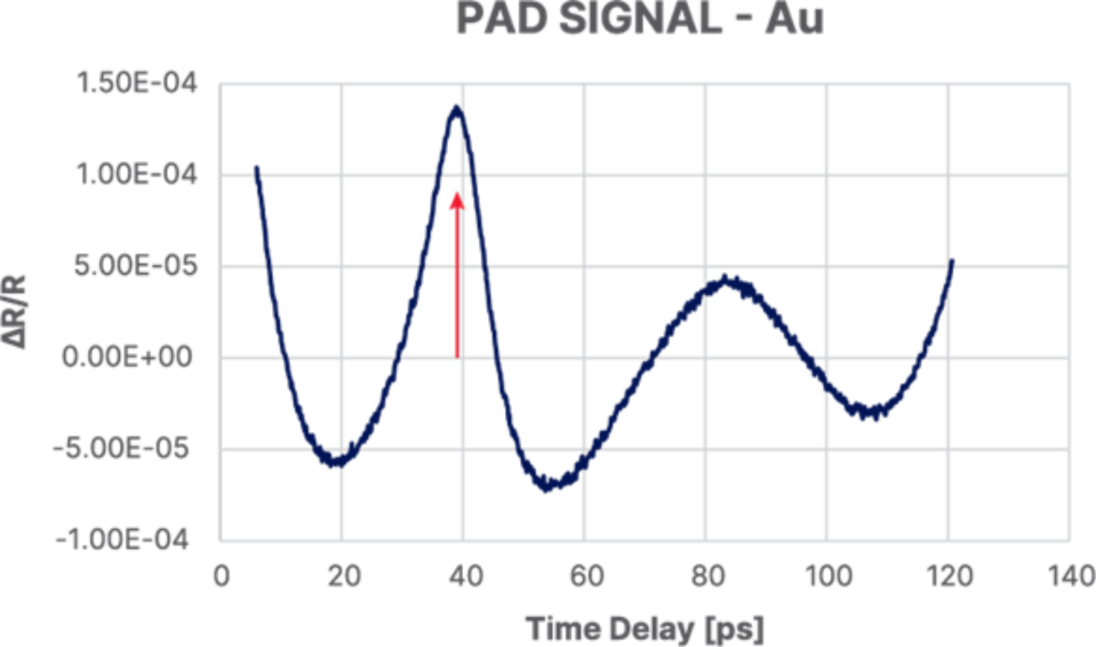
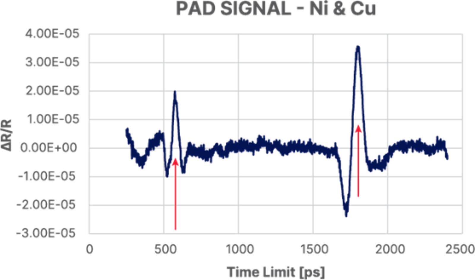
In Fig. 4 a-b, the red arrows indicate the reflectivity changes caused by the acoustic waves returning from the interface to the surface. With these peak positions, we were able to calculate each layer’s thickness with good accuracy and repeatability. The repeatability of Au, Ni and Cu films for each measurement was less than 0.2%, 0.05% and 0.05%, respectively. As such, all three film measurements outperformed the requirement of 10% gage repeatability and reproducibility.
It should be noted that Au film is much thinner than the other two films. As such, there is a significantly higher repeatability for Au films compared with the other films.
Conclusion
The AI era is upon us, and it would not be possible without advanced packaging innovations. However, the complexity of today’s advanced packaging is worlds away from traditional packaging. Today’s back-end process involves a variety of technologies and requires new methods of process control. In addition, controlling metal thickness and within wafer uniformity in these processes is critical to meeting the requirements for signal integrity in advanced packaging.
Unfortunately, some fabs still rely on legacy metrology tools like 4PP or contact profilometry—technologies that were never designed for the complexity of modern AI packages. These tools often introduce mechanical stress, lack the resolution to resolve thin or buried layers, and cannot reliably measure non-planar or dimpled structures.
As we have demonstrated, picosecond ultrasonic technology is an ideally suited interconnect metrology solution for both RDL and bond pads. This technology offers excellent accuracy and gage capability for the control of interconnect processes in advanced packaging.
As back-end processes demand the same level of precision, uniformity, and control traditionally associated with front-end requirements, picosecond ultrasonic technology can play a major role in advanced packaging metrology, delivering the non-contact, high-resolution, and repeatable measurements that AI applications demand.
Acknowledgments
We would like to thank Dae-Seo Park, Sanghyun Bae, Junghwan Kim, and Hwanpil Park of Samsung Electronics Co., Ltd., and Kwansoon Park, G. Andrew Antonelli, Robin Mair, Johnny Dai, Manjusha Mehendale and Priya Mukundhan of Onto Innovation for their contributions to this article.
About the author
Cheolkyu Kim, Ph.D., is director of product marketing at Onto Innovation with a focus on application development for picosecond ultrasonic (PULSE™) and inspection technologies. Prior to joining Onto, Kim was a postdoctoral research associate in the Physics Department of Brown University. During his three years at Brown, he spent time researching magnetically levitated superfluid liquid helium.
The 75th anniversary celebration of ECTC in Dallas showcases a remarkable evolution in advanced packaging technologies, revealing how semiconductor priorities have dramatically shifted. Rather than the relentless miniaturization of the smartphone era, today’s AI-driven applications demand larger packages with more functionality and sophisticated thermal management solutions.
Glass core substrates emerged as the star technology of the conference, with standing-room-only sessions demonstrating the industry’s intense interest in this promising material platform. The excitement is justified – glass offers superior dimensional stability and enables higher-density interconnects than traditional organic substrates. Meanwhile, co-packaged optics generated similar enthusiasm as engineers tackle the monumental challenge of powering AI server racks that consume between 0.5-1 megawatt each, making energy efficiency a critical concern.
The conversation with Onto Innovation’s Monita Pau begins at 1:10.
Yield Optimizer software is part of a comprehensive next-level data management portfolio. It reimagines manufacturing line control and analytics to explore the impact of previously invisible factors in day-to-day factory operation.
Yield Optimizer software is the next incarnation of analytics on the evolutionary scale. The software’s disruptive technology analyzes relationships between multivariant data and their complex interactions. By examining any set of conceivable inputs and outputs, Yield Optimizer software identifies the relationships and interactions that lead to positive operational changes. Easily understood visuals empower even casual users to understand what is important before making adjustments.
Yield Optimizer software evaluates multiple models and suggests the best one for the data. Using machine learning, it examines the interactions between in-process metrology readings and end-of-line test results for any semiconductor product family and recommends changes to the in-process metrology targets. When licensed as a service, it enables users to leverage an on-demand infrastructure to apply easily understood workflows for complex analytics without the overhead.
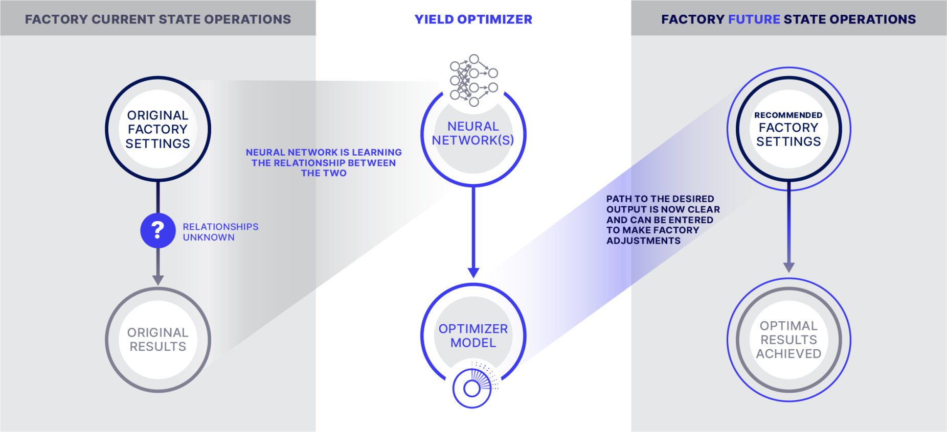
Neural networks model today’s data to achieve tomorrow’s in-line targets

Users across the fab benefit from Yield Optimizer software’s easy-to-apply analytics


As your partner for innovative solutions, we’re always here for you.
Discover how our cutting-edge semiconductor solutions are engineered to meet your most complex challenges: delivering performance, reliability and innovation where it matters most.
"*" indicates required fields