The demand for high bandwidth memory (HBM) is accelerating across the semiconductor industry, driven by boundary-pushing artificial intelligence, high-performance computing, and advanced graphics. These technologies require access to vast datasets, which in turn increases the need for memory solutions that combine speed, density, and power efficiency. HBM meets these demands by vertically stacking memory dies and linking them with ultra-fast interconnects.
With data rates rising, the need for increased output contact pad density is needed. To address this, bump technologies are being pushed beyond what was previously thought to be their physical and performance limits. As it stands today, some memory designers are innovating their way to bump sizes below 10µm in high volume manufacturing. Be that as may, scaling bump height to 2μm will be considerably challenging, leading some to explore hybrid bonding as an interconnect solution.
Hybrid bonding enables finer interconnect pitches of less than 10μm, allowing for more I/O terminals in a smaller area. This increased density translates directly into higher bandwidth and improved overall performance.
Traditional bump-based stacking introduces gaps of about 30μm between dies, while hybrid bonding offers direct Cu-to-Cu connections. By achieving near-zero spacing between dies, hybrid bonding significantly reduces overall package thickness and offers lower resistance and better thermal conductivity than bump-based methods. The result: improved signal integrity, reduced power consumption, and enhanced heat dissipation, each of which are critical for HBM.
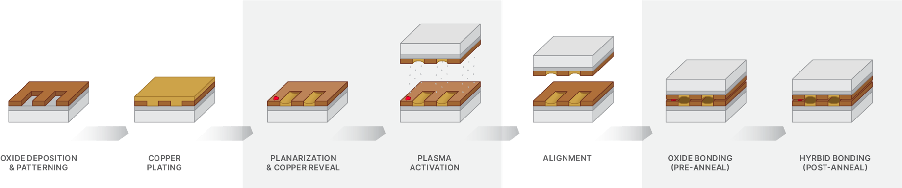
Finally, hybrid bonding supports several configurations: wafer-to-wafer, die-to-wafer, and die-to-die, offering flexibility in manufacturing and integration. This adaptability is vital for scaling HBM technologies across different applications and performance tiers.
Of course, hybrid bonding offers manufacturers its own set of challenges—increased sensitivity to particles and organic residues, lower yields and introduction of more costly process and process control steps—making the decision to stick to the tried-and-true microbump technology over the emerging, innovation a debate worth having.
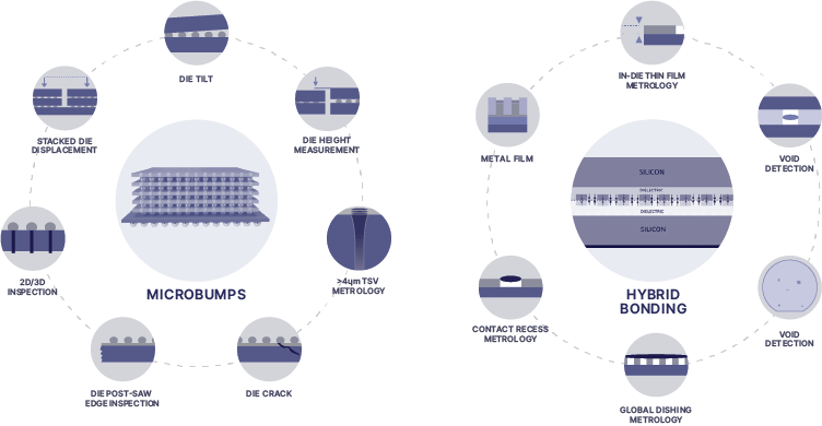
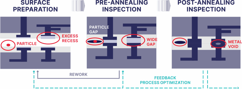
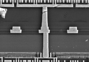
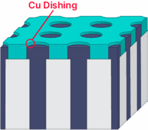
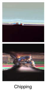
In this two-part blog series, we will compare these two interconnect solutions and discuss the challenges they face (Figure 1).
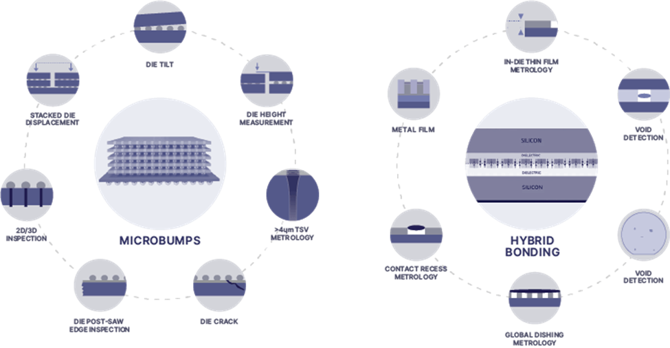
Figure 1: Interconnect challenges in microbump and hybrid bonding technologies.
Head to Head: Microbumps and Hybrid Bonding
Bumps have several advantages over hybrid bonding. As a mature technology, they are widely used and well-understood in the industry. They are also compatible with existing flip-chip and underfill processes, and are scalable for moderate density. In addition, the cost of bump technologies is lower than hybrid bonding technologies.
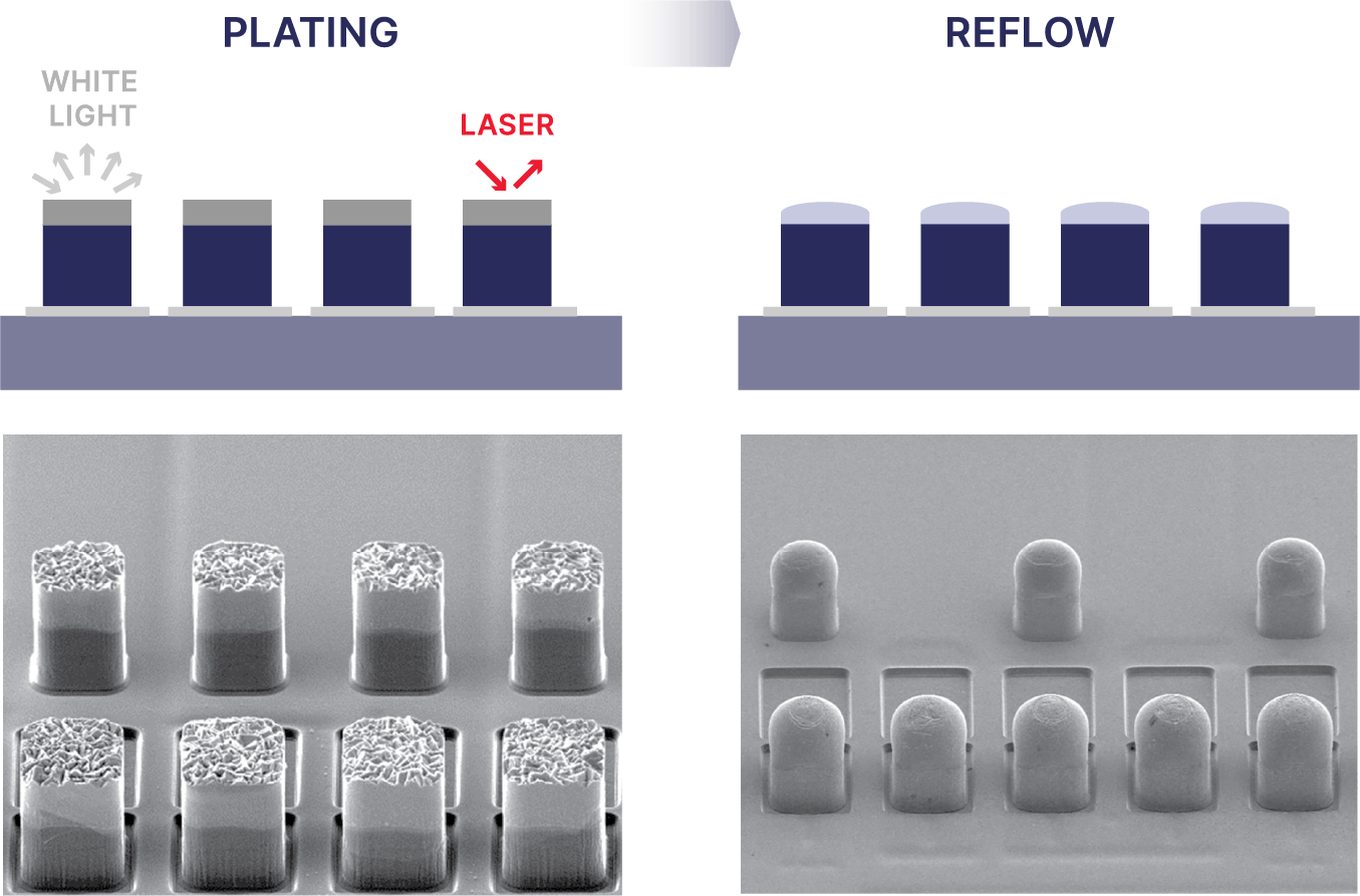
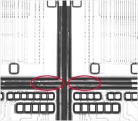
However, microbumps have a number of disadvantages compared to hybrid bonding. The most significant of which are the pitch limitations of bump technologies. Microbumps struggle at pitches below 10µm due to challenges in plating uniformity and solder reflow. Bumps also require underfill, which can introduce stress and complicate thermal management.
Limitations aside, bump technology continues to evolve. Leading suppliers of bump plating systems project a continued downscaling of bump dimensions, with diameters decreasing to the 5µm to 4µm range and heights dropping as low as 2µm to 1µm. At a 10µm pitch, the lateral footprint remains sufficient to support the high-density I/O requirements of advanced memory architectures. Concurrently, the reduced bump height enables vertical integration of up to 16 stacked HBM dies within the 775µm maximum package height defined by Joint Electron Device Engineering Council (JEDEC) standards. Consequently, bump interconnects remain a viable and scalable solution for next-generation HBM, and major manufacturers are maintaining substantial R&D investments in bump technology.
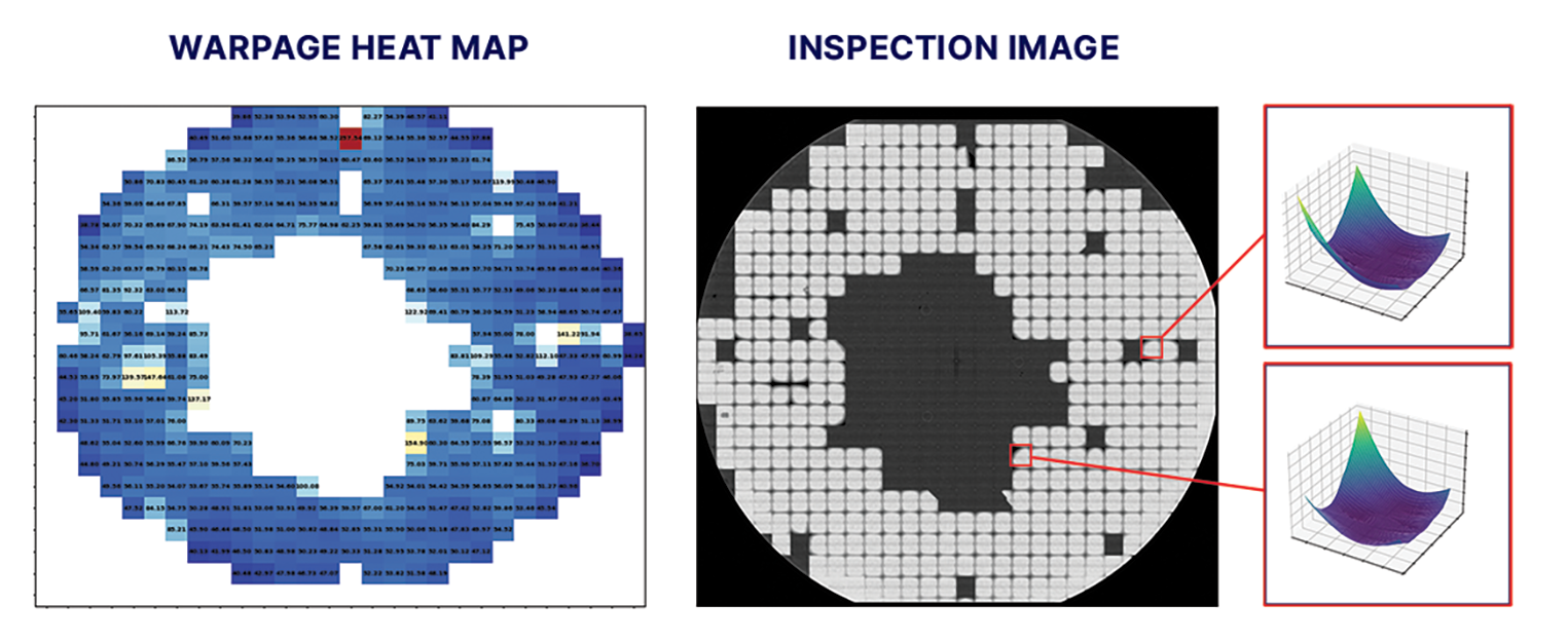
Hybrid bonding, while promising, presents its own set of challenges. Chief among them, hybrid bonding is especially sensitive to particles and organic residues; for example, even 1µm particles can cause defects. These residues can prevent proper contact, trap gases or moisture, and lead to void formation during bonding. Voids can cause delamination or incomplete bonding, reducing mechanical integrity and electrical continuity. Hybrid bonding also is more expensive than traditional bump technologies and may require manufacturers to purchase new equipment and adopt new process flows before moving away from bump technology.
Conclusion
As demand for HBM intensifies, the industry stands at a crossroads in interconnect technology. While microbumps have evolved to support increasingly dense and tall HBM stacks, they face several obstacles. Hybrid bonding offers a compelling alternative, but not without its own hurdles. Ultimately, both technologies are advancing in parallel, each with unique strengths and limitations.
Regardless of which interconnect technology is chosen, a comprehensive suite of interconnect solutions will be needed to address the obstacles manufacturers of HBM devices face. In the second in this two-part series, we will explore a number of these solutions that, when combined, tackle the biggest challenges facing interconnects in HBM.
Biography
Damon Tsai joined Onto Innovation in 2018 and has extensive experience in inspection and metrology, with a specialized focus on semiconductor FEOL, advanced packaging, OSAT, and specialty markets like RF, Power, and CIS. He currently serves as the Senior Director of Product Marketing, Inspection.
Woo Young Han joined Onto Innovation in 2000 and is currently Product Marketing Director, Inspection. He holds an Electrical Engineering degree from University of Toronto.
Tim Kryman is Product Marketing Senior Director, Metrology and Inspection. Tim has been with Onto Innovation for more than 20 years and holds a BS in Accounting and Information Systems from Lock Haven University and an MBA from DeSales University.