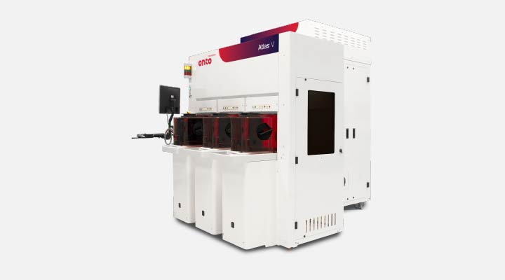
Atlas® V System

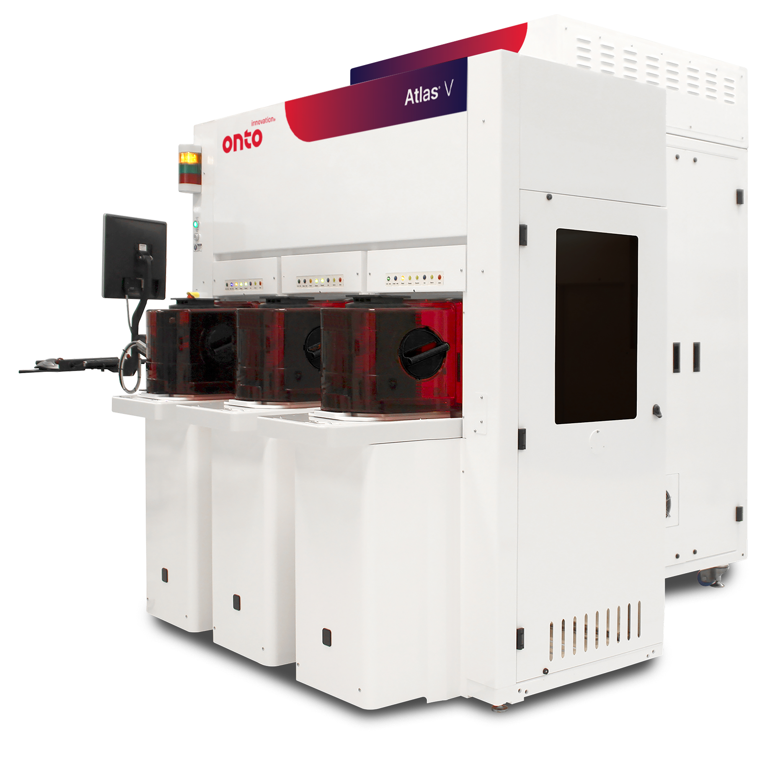
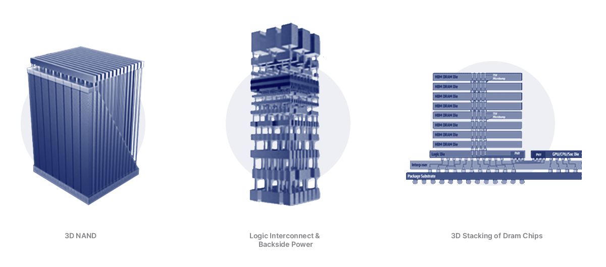
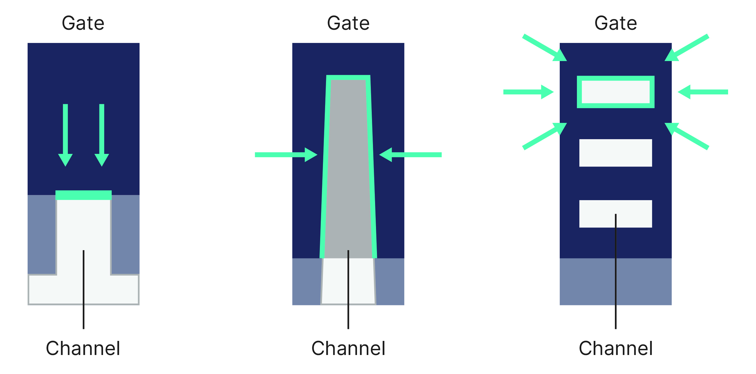
The Atlas V system is an OCD and thin film metrology tool for high volume manufacturing, enabling FinFET & Gate-All-Around (GAA) logic, DRAM, and 3D NAND device process control.

Atlas® V System

Product Overview

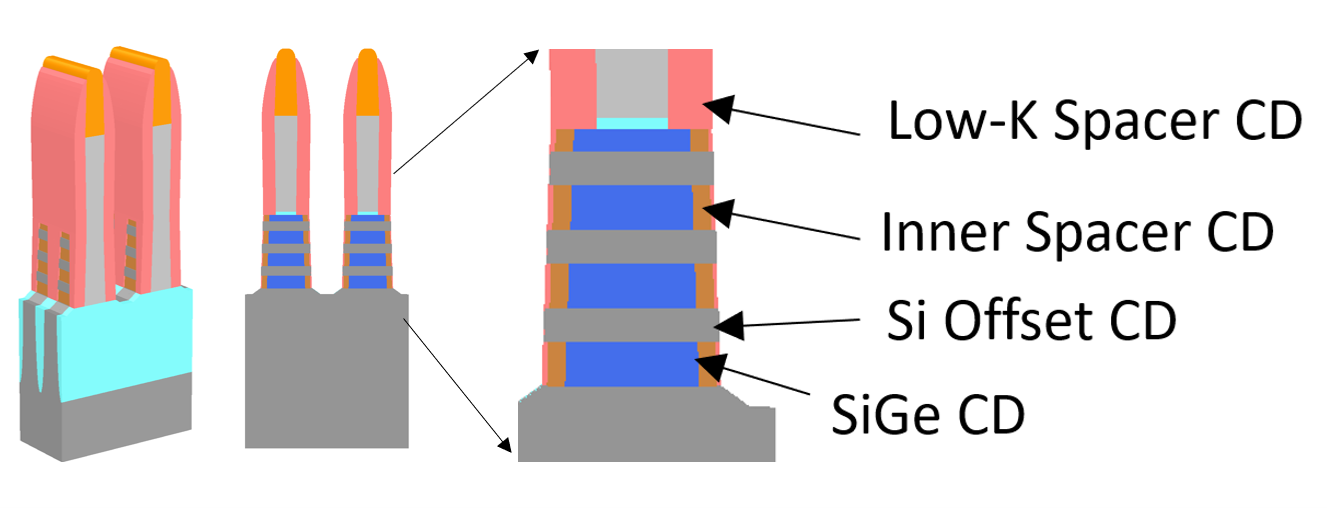
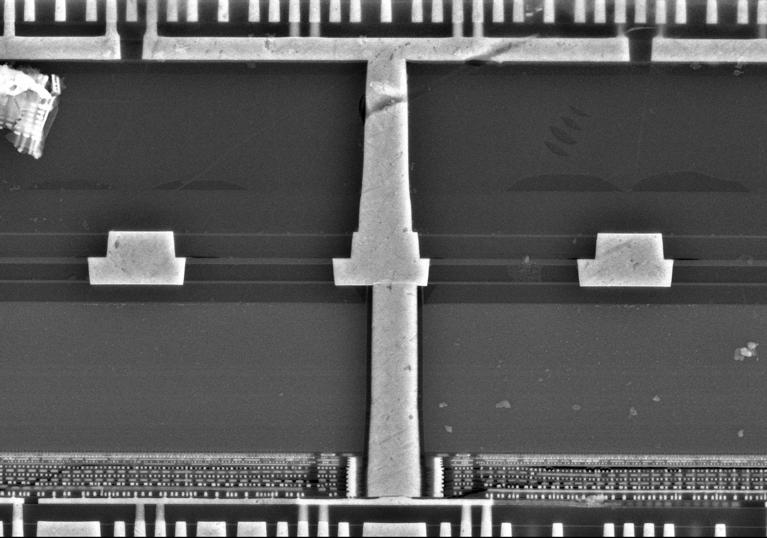
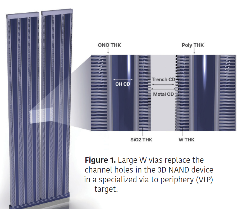
The Atlas V system combines state of the art optical design with an innovative Ai Diffract modeling engine, providing OCD and thin film metrology solutions for measuring complex 3D device structures. The dual channel optical architecture consists of a DUV 4×4 Mueller Matrix (MM) SE and a DUV polarized normal incident reflectometer (NIOCD). Together, they provide rich information for OCD analysis at high precision and high throughput. The Atlas V system is designed to measure the most critical and challenging process steps that include buried features, not visible by CD-SEM and other techniques.

With unique capabilities, such as measuring individual nanowire dimension in a GAA logic device, the Atlas V system is an enabling technology for leading edge device process control.

Applications

  • OCD for litho, etch, CVD & CMP process in all device segments
  • Local variation
  • Asymmetry and tilt
  • Common and critical films
  • Stress & wafer warpage
Related Products
View all
Atlas-G6-NEWBRAND-featured-720×400

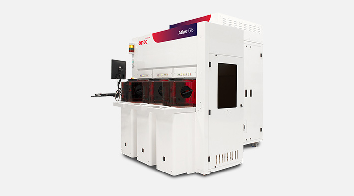
Atlas® G6 System

Leading edge OCD and thin film metrology for next-generation AI applications and beyond.
View Product
atlasiii_feat

Atlas® III+ System

Versatile OCD and thin film metrology for mature and mainstream nodes.
View Product
impulse v_feat

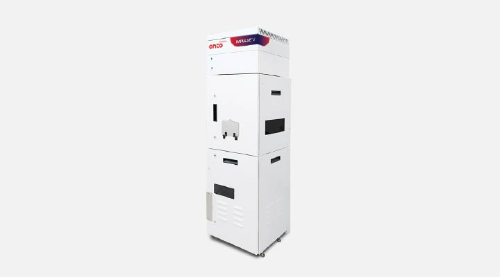
IMPULSE® V System

Advanced high throughput integrated metrology system with AI-driven machine learning option. The system offers maximum sensitivity and accuracy to CMP process excursions and enables process engineers to establish APC control with high-accuracy feedback.
View Product
impulse+_feat

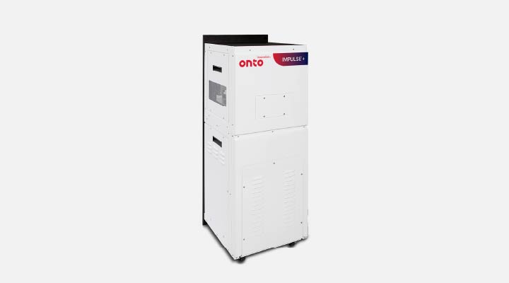
IMPULSE®+ System

Integrated metrology system offering maximum sensitivity and accuracy to CMP process excursions and enabling process engineers to establish APC control with high-accuracy feedback.
View Product
aspect_feat

Aspect® System

Advanced infrared optical critical dimension (IRCD) metrology system for high aspect ratio structures in 3D NAND, 2D & 3D DRAM, CIS and power devices.
View Product
ocdsolutions_aidiffract_feat

OCD Solutions

A suite of OCD modeling software and computing hardware offering comprehensive capabilities for inline metrology, offline recipe creation and fleet management.
View Product
Related Insights & Resources
View all
mid-infared

Mid-infrared ellipsometry for optical critical dimension metrology

Learn more
impulse-1-duo

Enhancing CMP Process Control with Intelligent Line Monitoring & Integrated Metrology

Learn more
high-profile-dram

Non-destructive Metrology Techniques for Measuring Hole Profile in DRAM Storage Node

Learn more
GAA

Optical Critical Dimension Metrology for Semiconductor Manufacturing

Learn more
fig-1_200720_065724

Metrology Solutions for Gate-All-Around Transistors in High Volume Manufacturing

Learn more

Do you have an Atlas V system question? Let’s talk!

As your partner for innovative solutions, we’re always here for you.

Discover how our cutting-edge semiconductor solutions are engineered to meet your most complex challenges: delivering performance, reliability and innovation where it matters most.

Let’s Talk

"*" indicates required fields

This field is for validation purposes and should be left unchanged.

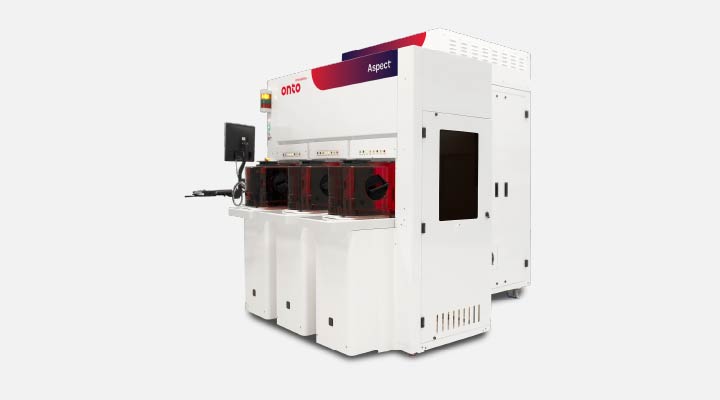
Aspect® System

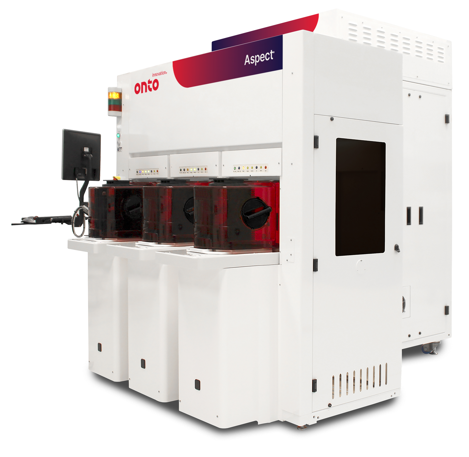
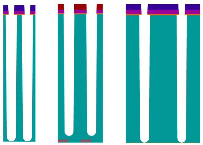
The Aspect System is a revolutionary in-line, non-destructive infrared optical critical dimension (IRCD) system measuring Z-dimension profiling of high aspect ratio structures to enable critical process control. It meets the needs of leading-edge customers with its high speed and process coverage.

Aspect® System

Product Overview

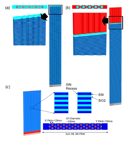
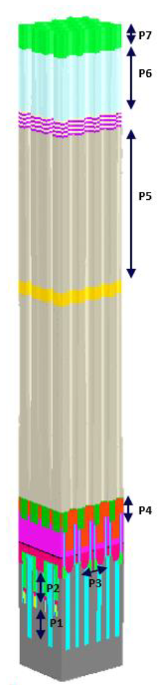
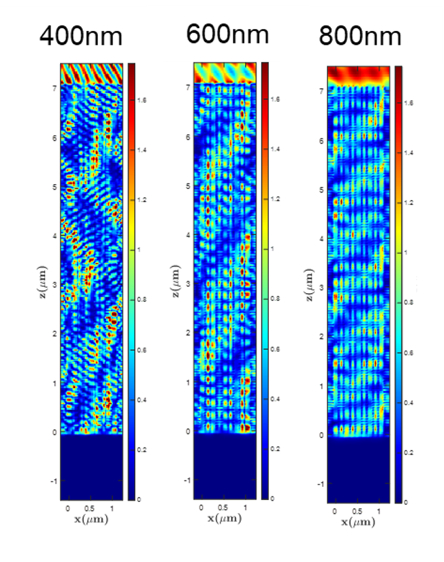
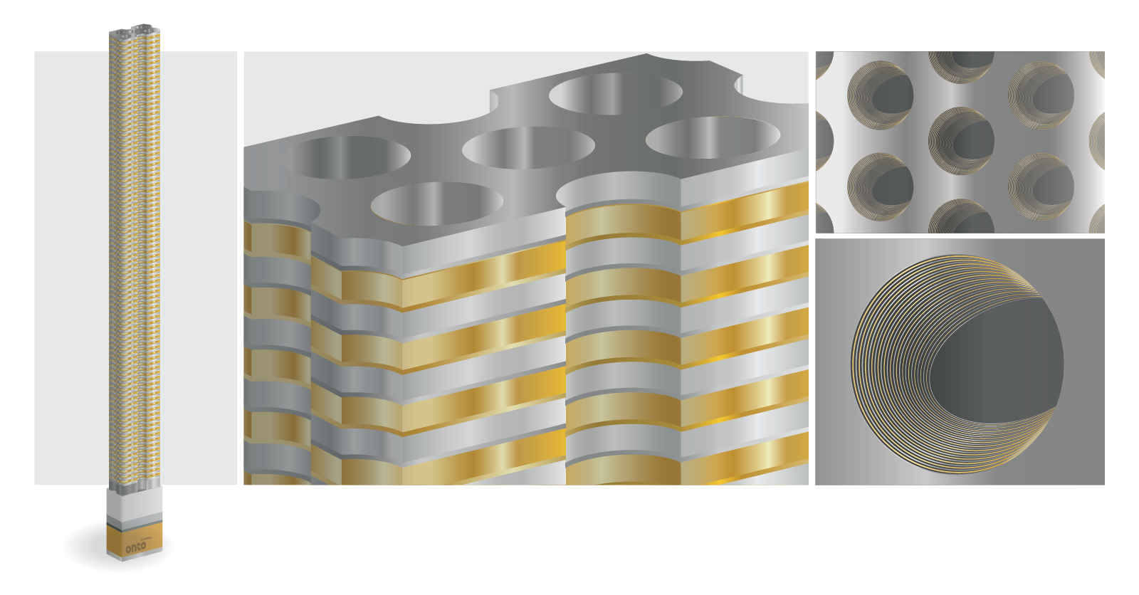
As the semiconductor industry relentlessly pursues density and power scaling, more and more high aspect ratio (HAR) processes are used across multiple device segments, especially in advanced memory such as 3D NAND and 3D DRAM. The Aspect metrology system was designed with these ongoing architectures and scaling strategies in mind. Aspect metrology has demonstrated superior performance across multiple customer devices through a unique proprietary IRCD system that provides full profiling capability to enable critical process control, with the speed and process coverage that customers require.

The Aspect system is powered by a software analysis engine, Ai Diffract™, that provides up to 90% faster time to solution which extends the industry leading NanoDiffract® software by leveraging extensive machine learning capabilities along with high fidelity modeling. The result is a simultaneous improvement in metrology performance along with a significant time to solution reduction.

Applications

  • Etch, cleans, and deposition for 3D NAND
  • Etch, cleans, and deposition for 2D and 3D DRAM
  • Deep trench etch and doping for CIS
  • Deep Trench etch in Power Devices
  • On-device materials characterization for EPI process
Related Products
View all
atlasv_feat

Atlas® V System

High performance OCD and thin film metrology for advanced GAA and memory devices.
View Product
atlasiii_feat

Atlas® III+ System

Versatile OCD and thin film metrology for mature and mainstream nodes.
View Product
element s_feat

Element™ S System

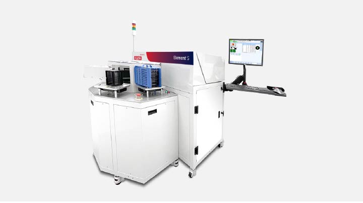
Transmission and reflection combined FTIR Measurement for wafer, specialty devices, supporting 100-200mm wafer sizes.
View Product
elementg2_feat

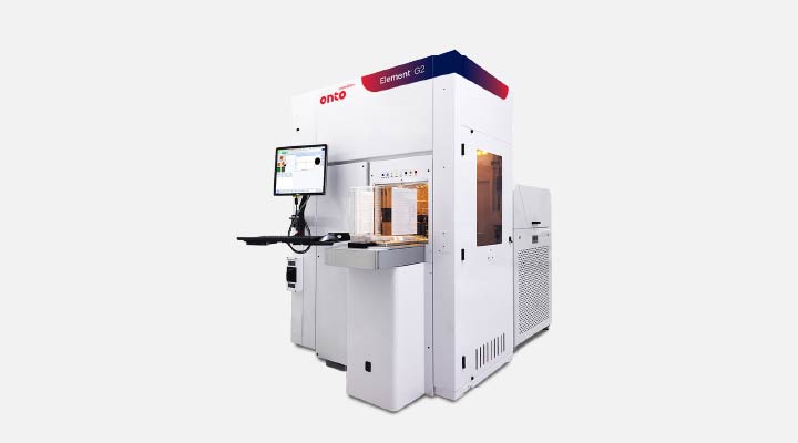
Element™ G2 System

Transmission and reflection combined FTIR measurement for advanced epi thickness, film composition control and advanced IR modeling.
View Product
Aspect S System _feat

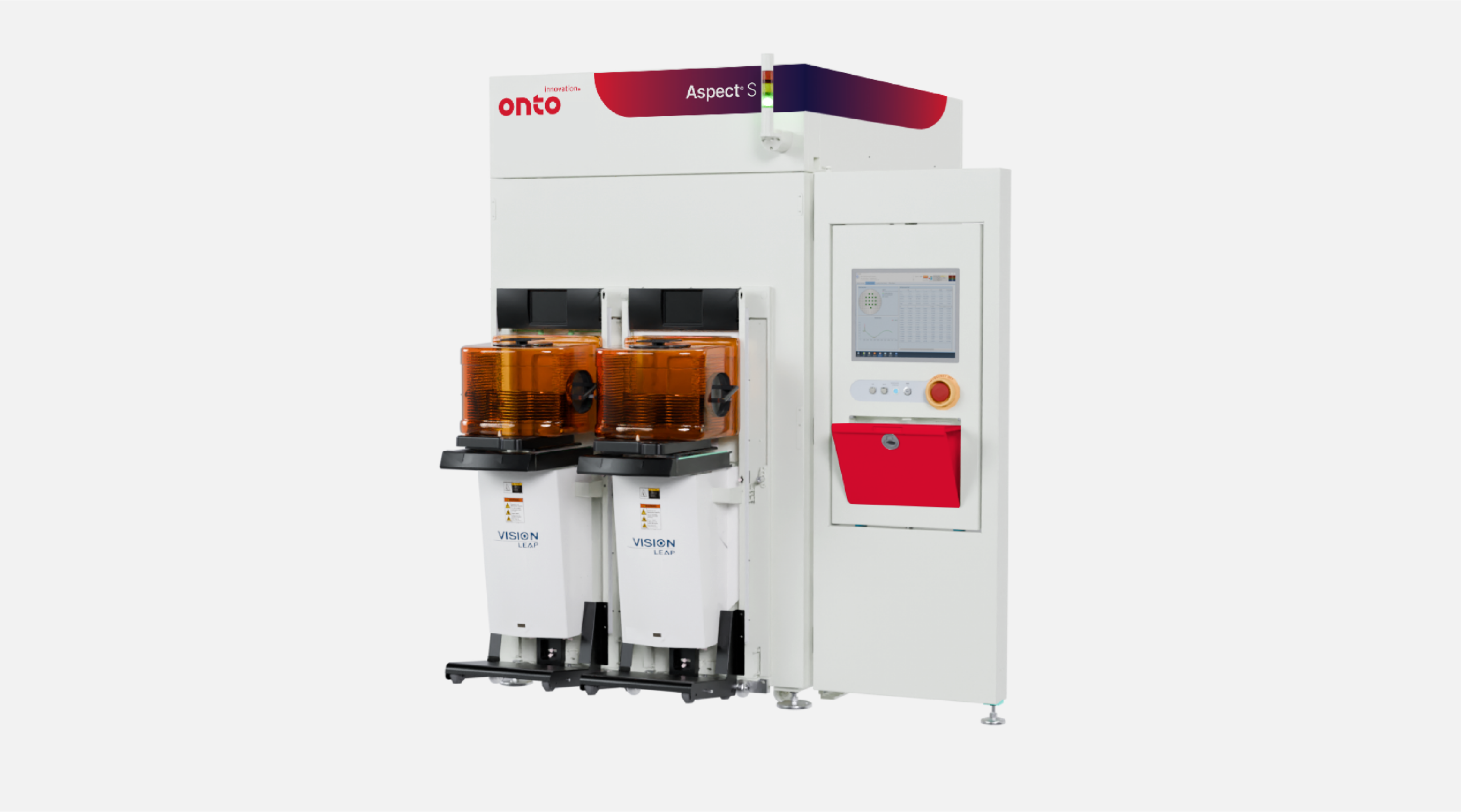
Aspect S System 

Advanced model-based infrared reflectometry (MBIR) metrology system for in-line monitoring of 3D structures used in V-NAND, CIS and power devices, as well as carbon hardmasks, dielectric compositions and epitaxial layer stacks.
View Product
Related Insights & Resources
View all
mid-infared

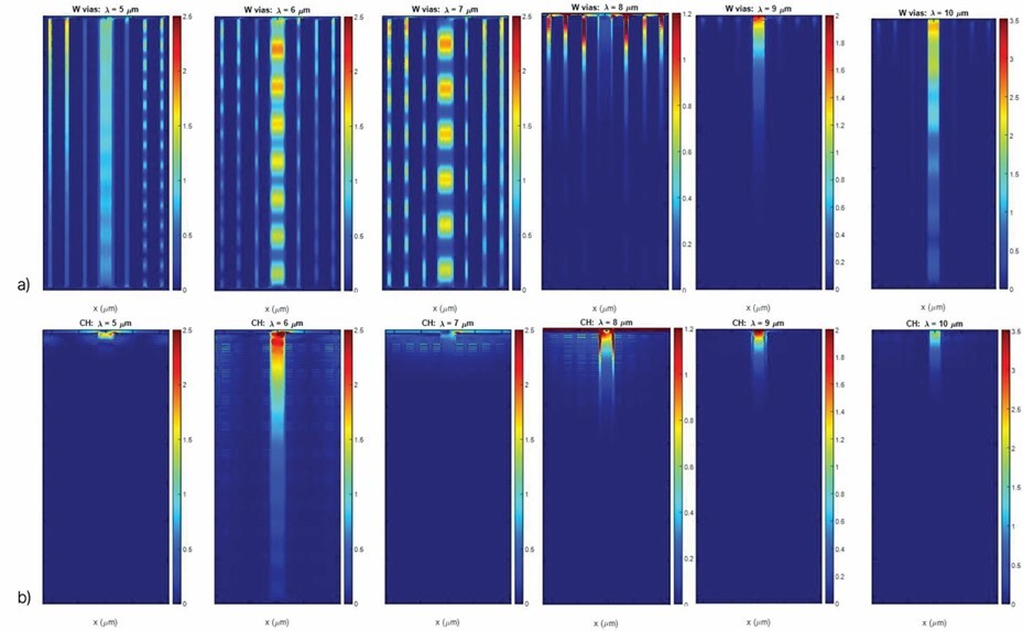
Mid-infrared ellipsometry for optical critical dimension metrology

Learn more
Deep-trench

Non-destructive Measurement of Bottom Width in Deep Trench Isolation Structures Using IRCD Metrology

Learn more
new-technique

Measuring the Critical W-recess in 3D NAND

Learn more
IRCD_220208_132903

Critical Moves: Advanced Logic Devices And CIS Benefit From Applications Using IRCD Metrology

Learn more
aspect-social

Mid-Infrared Optical Metrology for High Aspect Ratio Holes in 3D NAND Memory Manufacturing

Learn more
3D-Nand2

Untangling 3D NAND: Tilt, Registration, and Misalignment

Learn more

Do you have an Aspect system question? Let’s talk!

As your partner for innovative solutions, we’re always here for you.

Discover how our cutting-edge semiconductor solutions are engineered to meet your most complex challenges: delivering performance, reliability and innovation where it matters most.

Let’s Talk

"*" indicates required fields

This field is for validation purposes and should be left unchanged.

NovusEdge® G2 System

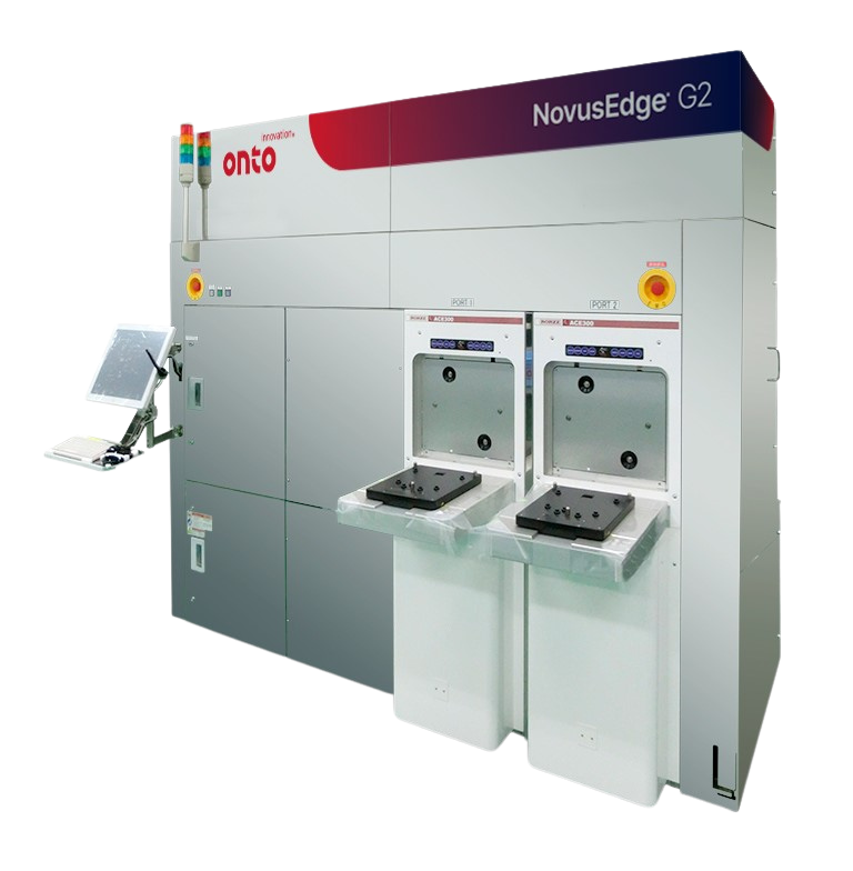
The NovusEdge G2 System offers fast, reliable edge, notch and backside inspection for 300mm unpatterned wafers, utilizing modular configurations.

NovusEdge® G2 System

Product Overview

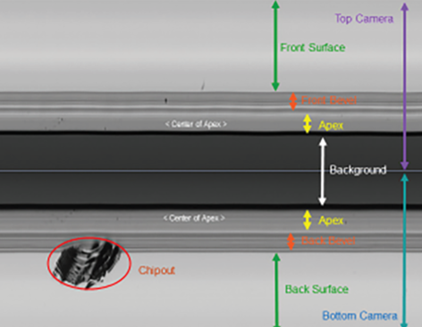
The NovusEdge G2 System provides high sensitivity inspection for the edge and backside of unpatterned wafers for current and advanced nodes. Configurable modules on the same automation platform increase throughput while maintaining a small footprint for improved cost of ownership. The edge-gripping handling solution for both automation platform and the inspection modules provide desired cleanliness required for manufacturing. Optional high-sensitivity notch inspection can be added. Defects are automatically classified and binned at run time to reduce manual review.

Designed as a multipurpose inspection and sorting system for end of line outgoing quality inspection of 300mm unpatterned wafers, the system identifies, inspects and sorts wafers according to recipes.

The NovusEdge G2 system offers higher sensitivity than the previous generation, with sub-micron resolution and increased throughput by over 15%. User interaction is simplified, and the new electrical design consumes less power.


Applications

  • In-process unpatterned wafer sorting (grading)
  • Incoming wafer inspection
  • Tool qualification and monitoring
Related Insights & Resources
View all
mystery

A Bare Wafer Mystery: Inspecting for Back, Edge and Notch Defects in Advanced Nodes

Learn more
Hunting-Image

Hunting For Macro Defects: The Importance Of Bare Wafer Inspection

Learn more

Do you have a NovusEdge G2 system question? Let’s talk!

As your partner for innovative solutions, we’re always here for you.

Discover how our cutting-edge semiconductor solutions are engineered to meet your most complex challenges: delivering performance, reliability and innovation where it matters most.

Let’s Talk

"*" indicates required fields

This field is for validation purposes and should be left unchanged.