
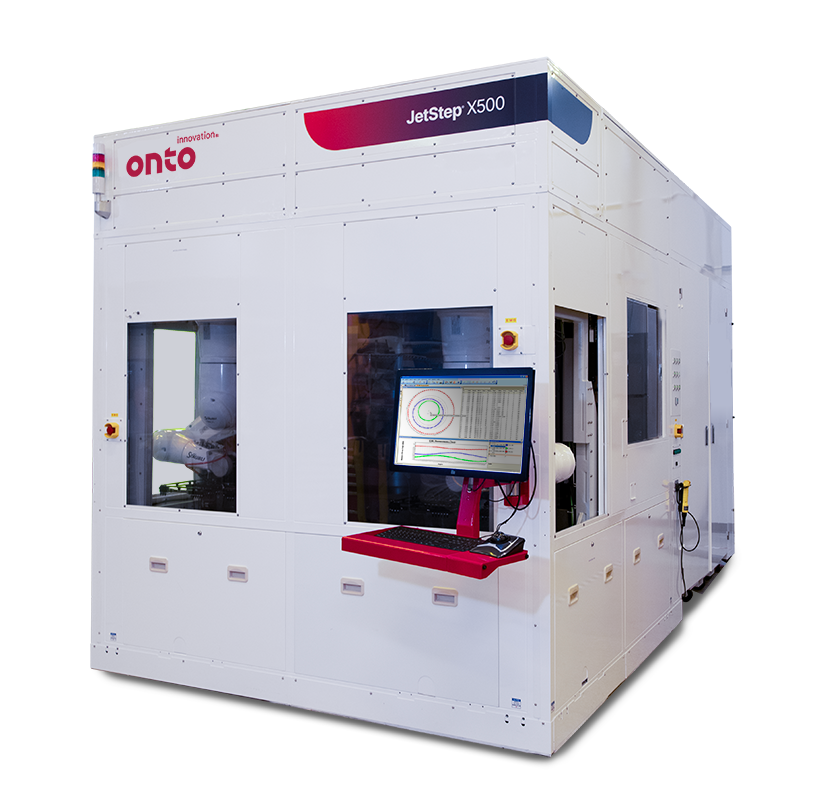
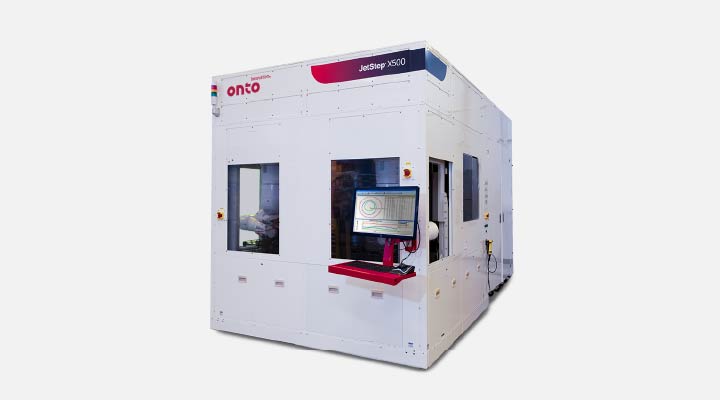
JetStep® X500 System
The JetStep X500 system is designed to provide AICS and OSAT manufacturers with a high-volume manufacturing lithography solution for heterogeneous integration. The JetStep X500 system exposes panel-type substrates made of CCL, FR4, composite, glass or other materials.
Product Overview
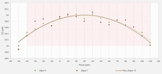
The JetStep X500 panel lithography system is optimized for high volume manufacturing of high-end AICS and other advanced packaging panel applications. As we approach the limits of Moore’s law, the JetStep X500 system addresses the need for extremely large packages integrating multi-node chips, or “chiplets,” enhancing functionality, speed, I/O count and reducing power consumption for server farms, AI, and mobile applications. The JetStep X500 system features the industry’s largest exposure field , fine line RDL resolution with large depth of focus (DOF), excellent overlay accuracy, and automatic magnification compensation with independent x and y magnification adjustment. The JetStep X500 system handles a large range of substrate thicknesses with high levels of warp, offering unique imaging parameter control to compensate for panel distortion. Additionally, it can run highly warped substrates with an edge clamping option and provides real-time autofocus at every exposure site to compensate for challenging topography.
Applications
- AICS
- Fan-out panel level packaging (FOPLP)
- Large package formats, exposed without stitching
- Large interposers
- Redistribution layer (RDL) / underbump metallization (UBM)
- Vias in photo imageable dielectric (PID)
Featured Markets


Adaptive Shot Lithography Solution
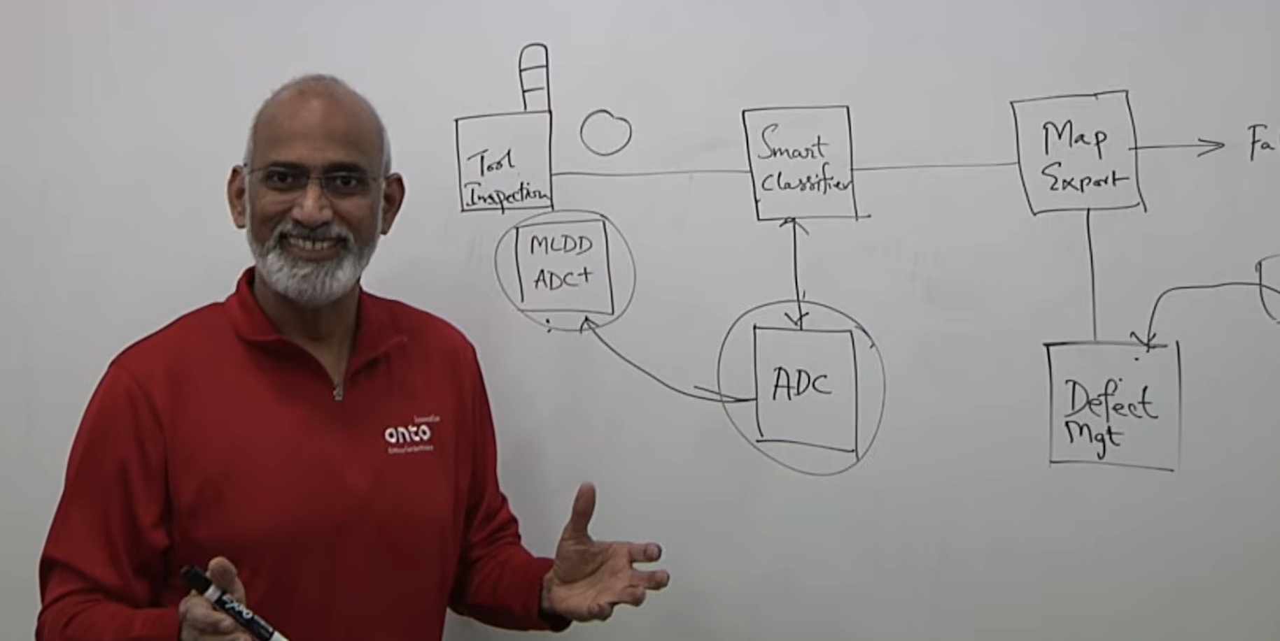
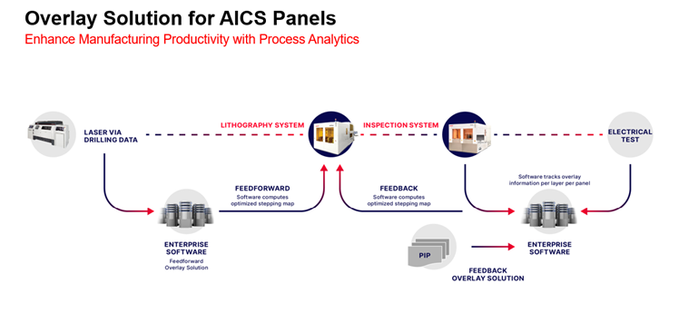
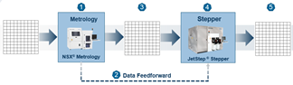
Die shift on reconstituted panels can significantly impact both productivity and yield. To address this challenge, we use a parallel die placement measurement process and advanced analytics to provide a means to balance productivity against yield. Our integrated lithography cell, featuring Firefly inspection, StepFAST software, and JetStep Lithography, delivers industry-leading throughput and yield for fan-out panel level packaging.
Overcoming FOPLP Die Placement Error
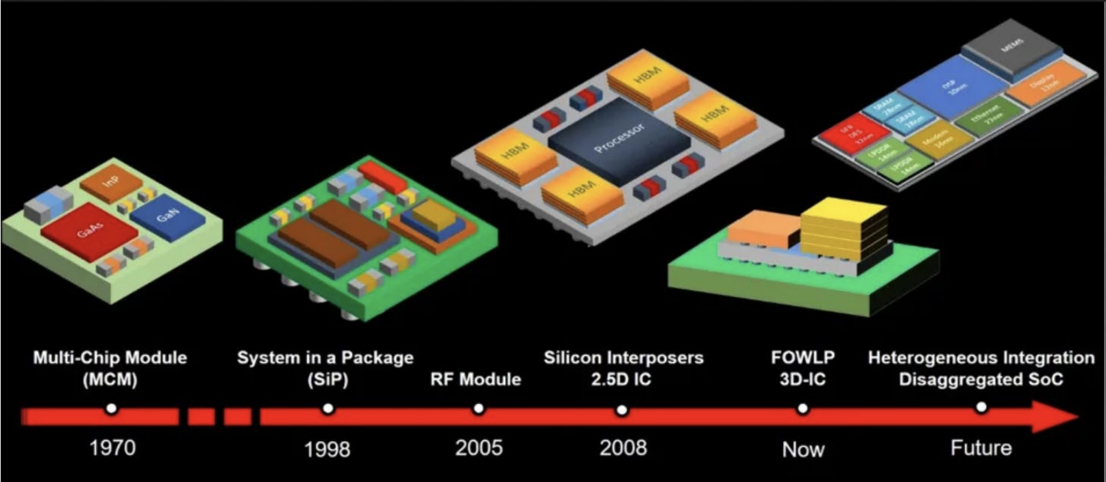
It is well understood that advanced packaging applications require high performance, low cost, increased functionality and improved reliability that 2.5D and 3D packaging solutions provide. Fan-out panel-level packaging (FOPLP) is one of the technologies that has the potential to meet these packaging requirements.
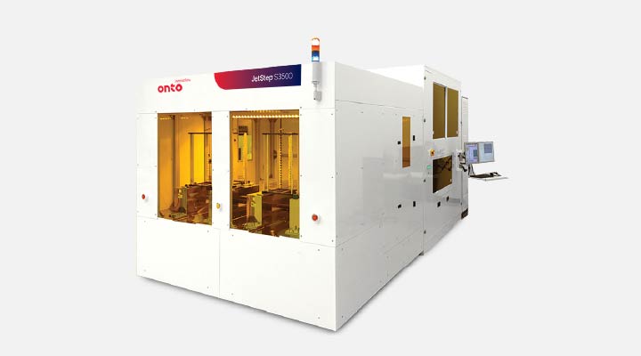
JetStep® S3500 System
The JetStep S3500 system is designed to provide OSATS with a high-volume manufacturing advanced packaging lithography solution. For substrates up to 720mm x 600mm, it supports fan-out panel level packaging.
JetStep® X500 System
The JetStep X500 system is designed to provide AICS and OSAT manufacturers with a high-volume manufacturing lithography solution for heterogeneous integration. The JetStep X500 system exposes panel-type substrates made of CCL, FR4, composite, glass or other materials.
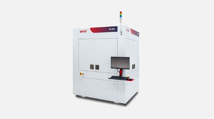
Firefly® G3 System
The Firefly G3 system provides automated inspection and 3D metrology for advanced IC substrates and panel level packaging, delivering high resolution and productivity for demanding applications like high-performance computing (HPC), artificial intelligence (AI), cloud computing and machine/deep learning.

StepFAST® Software
An advanced feed-forward lithography software solution for fan-out panel level packaging that enhances yield and throughput by correcting die placement errors through external measurements, predictive analytics and adaptive shot control.
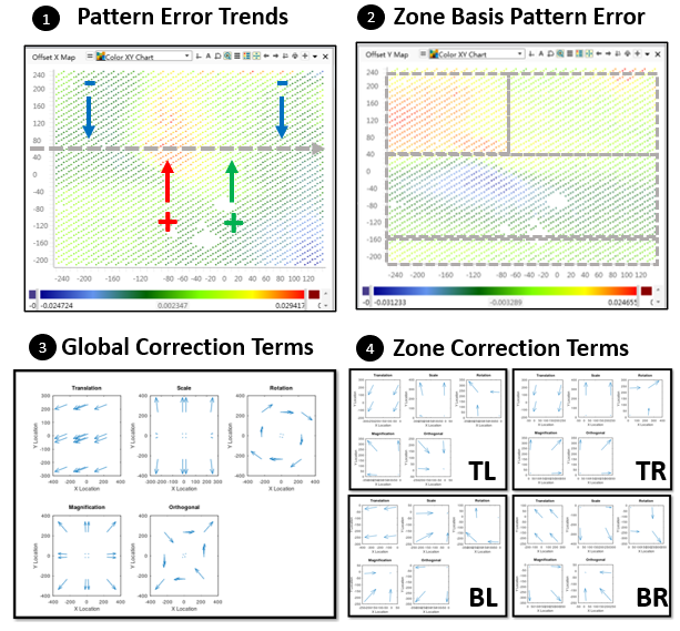
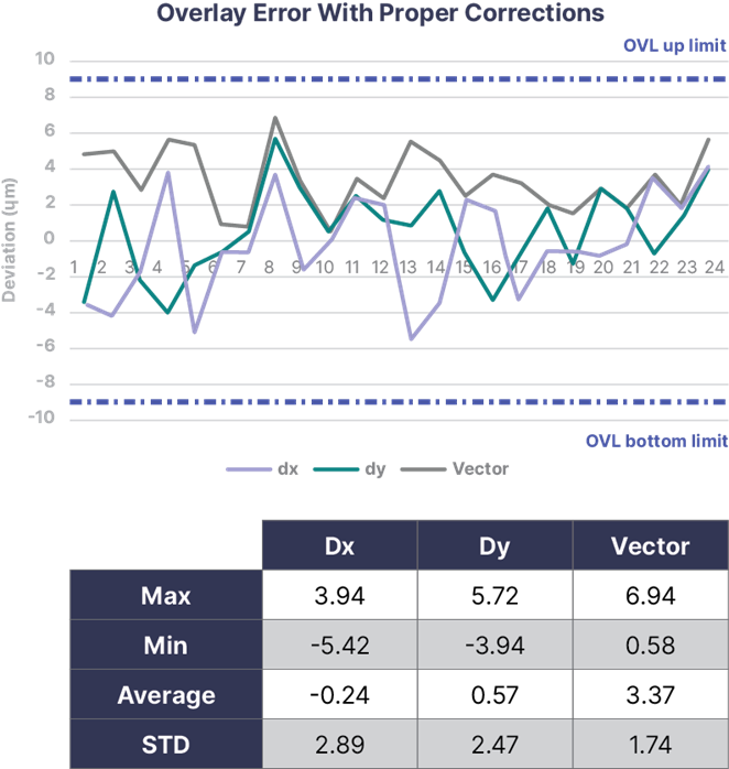
Adaptive Overlay Control
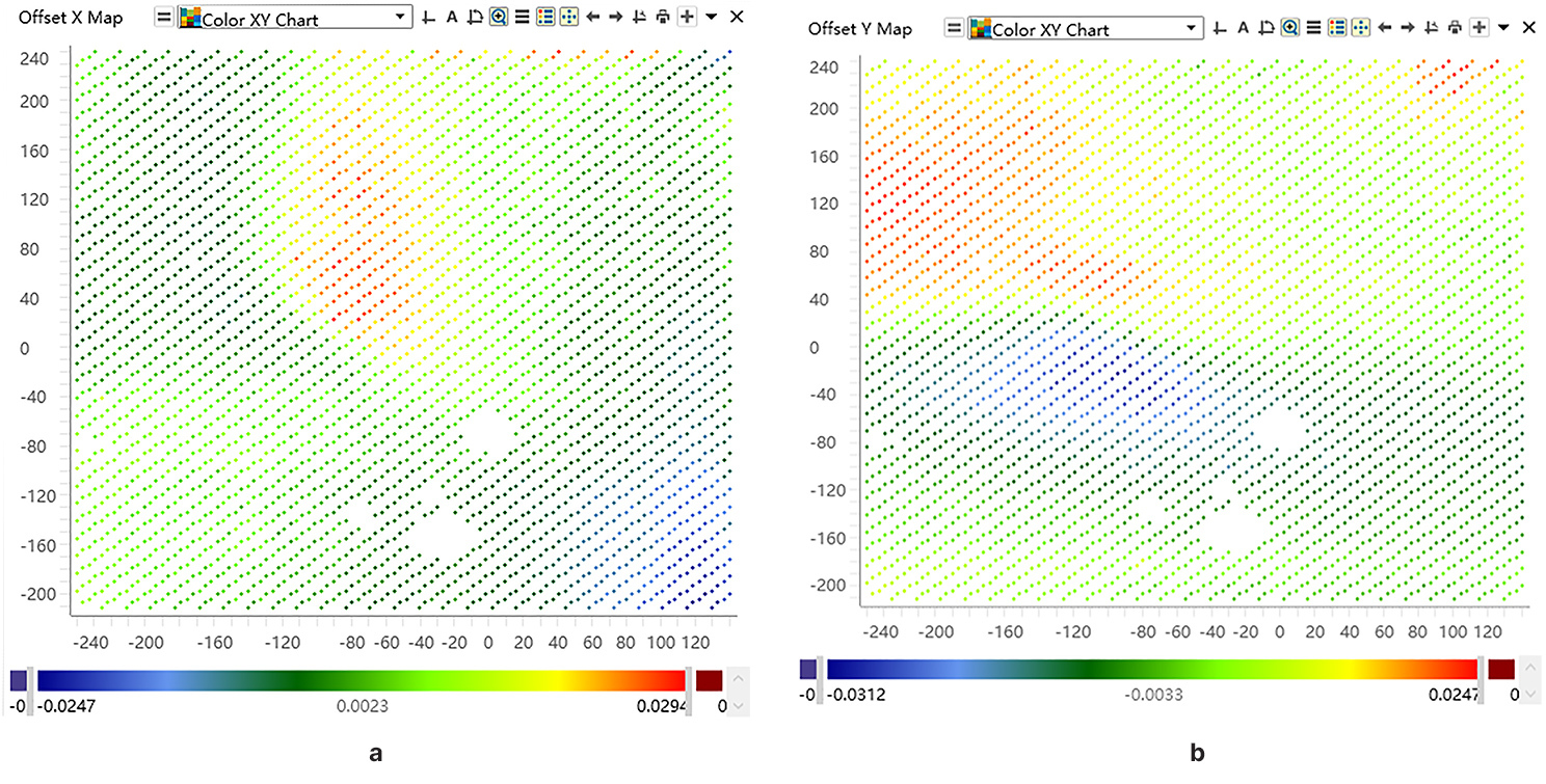
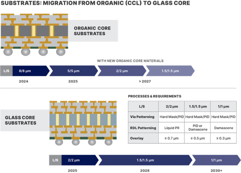
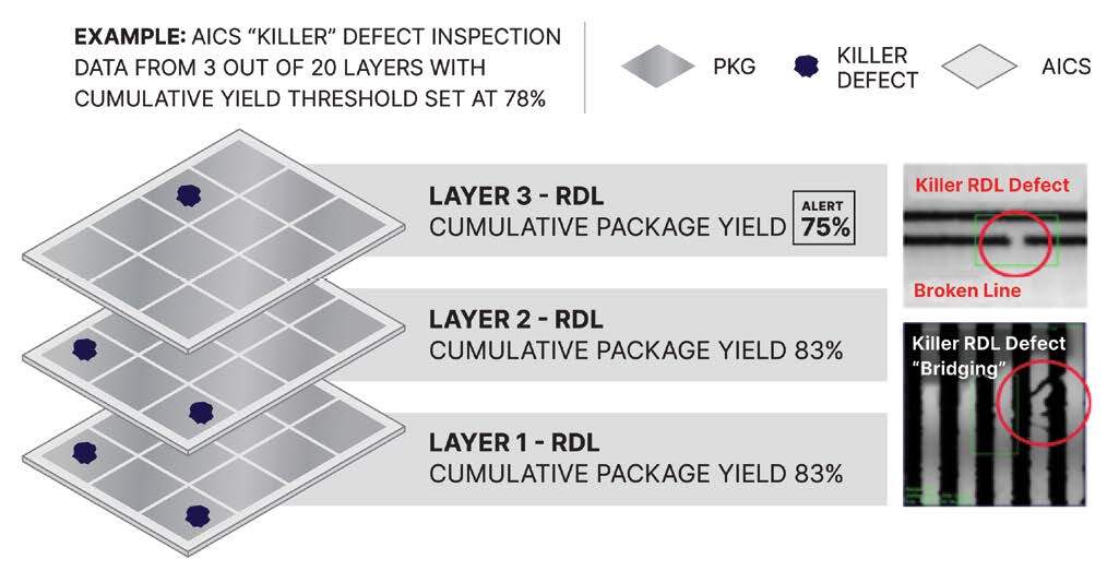
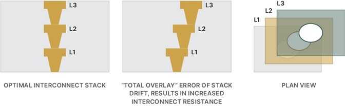
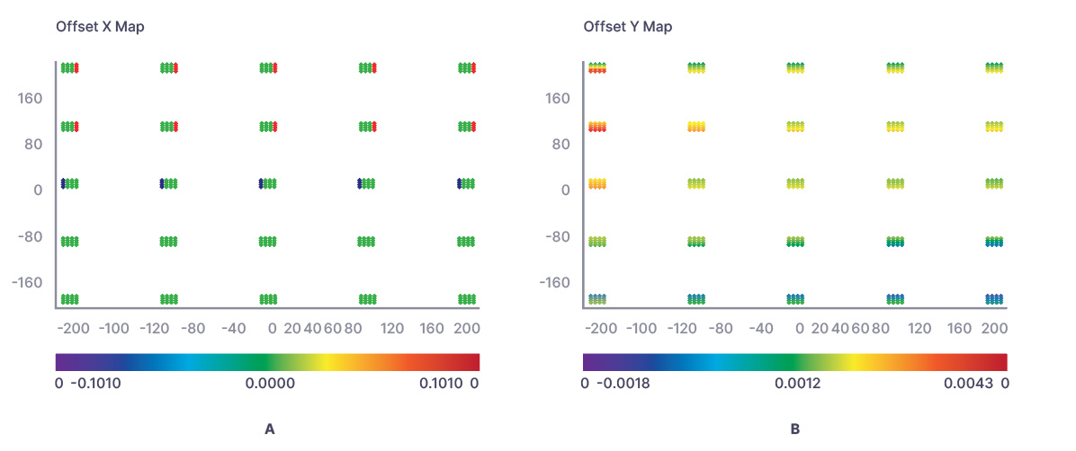
During the processing of organic (CCL) advanced IC substrates (AICS) the substrates become distorted which impacts the overlay of Via to RDL pad structures. To solve this problem, the stepper must adjust the alignment solution to match the previous layer’s distortion by measuring the overlay. Proprietary software provides the user with the ability to adjust each zone of the AICS with independent offsets.
Analysis of Pattern Distortion by Panel Deformation
The growing demand for heterogeneous integration is driven by the 5G market. This includes smartphones, data centers, servers, high-performance computing (HPC), artificial intelligence (AI) and internet of things (IoT) applications. Next generation packaging technologies require tighter overlay to accommodate larger package sizes with fine-pitch chip interconnects on large-format flexible panels.
JetStep® X500 System
Designed for advanced IC substrates (AICS), it incorporates a large field exposure area with a large depth of focus. Proprietary software enables independent zone offset adjustments across the AICS.
Firefly® G3 System
The Firefly G3 system provides automated inspection and 3D metrology for advanced IC substrates and panel level packaging, delivering high resolution and productivity for demanding applications like high-performance computing (HPC), artificial intelligence (AI), cloud computing and machine/deep learning.
JetStep® S3500 System
StepFAST® Software
Early Zone Correction for Enhanced Overlay Precision in Next-Generation FOPLP Lithography
Yield Prediction Technology: A Game Changer for Cutting Costs and Reducing Ramp Time in FOPLP Lithography
The Innovations Driving the Advanced Packaging Roadmap, Part 1

Onto Innovation’s PACE Partners Talk About Collaborating on Panel-Level Packaging
Picking up the Pace of Panel-level Advanced Packaging at Onto Innovation
Overlay Optimization In Advanced IC Substrates

How AI is Helping Optimize AI Chip Production
The Great Lithography Debate: Copper Clad Laminate or Glass Substrates?
Optimizing Advanced IC Substrates (AICS) for PLP
Total Overlay With Multiple RDLs with Keith Best

The Glass Substrate Question: When Will It Replace Copper Clad Laminate?
Addressing Copper Clad Laminate Processing Distortion Using Overlay Corrections
Addressing Total Overlay Drift In Advanced IC Substrate (AICS) Packaging
Heterogeneous Integration: Correcting Overlay Errors On Advanced Integrated Circuit Substrates (AICS)
Heterogeneous Integration: Exposing Large Panels with Fewer Shots
‘XL’ Fine Resolution Large Field Lithography Dramatically Cuts FOPLP Pattern Distortion
Analysis of Pattern Distortion by Panel Deformation and Addressing it by Using Extremely Large Exposure Field Fine-Resolution Lithography
Outlier Control Technology and Feedforward Lithography Can Boost FOPLP Yield
Large-field, Fine-resolution Lithography Enables Next-generation Panel-level Packaging
Extremely Large Exposure Field With Fine Resolution Lithography Technology To Enable Next Generation Panel Level Advanced Packaging
Advanced Outlier Die Control Technology in Fan-Out Panel Level Packaging Using Feedforward Lithography
Adaptive Shot Technology To Address Severe Lithography Challenges For Advanced FOPLP
Overcoming FOPLP Die Placement Error

Do you have a JetStep X500 question? Let’s talk!
As your partner for innovative solutions, we’re always here for you.
Discover how our cutting-edge semiconductor solutions are engineered to meet your most complex challenges: delivering performance, reliability and innovation where it matters most.
Let’s Talk
"*" indicates required fields