Lithography

Advanced packaging steppers designed to tackle manufacturing challenges, maximizing throughput while ensuring high resolution and precise overlay.

Jump to:

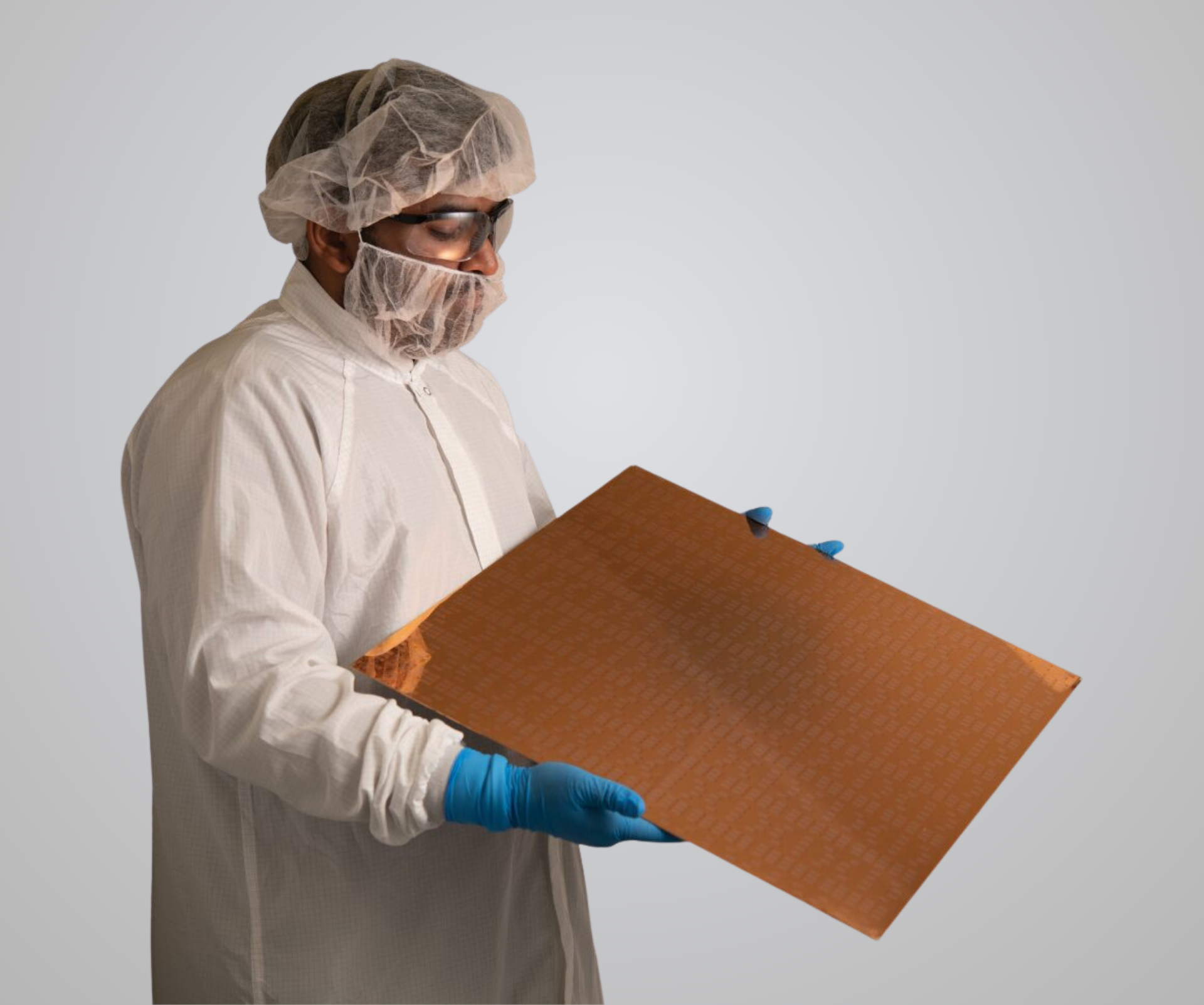
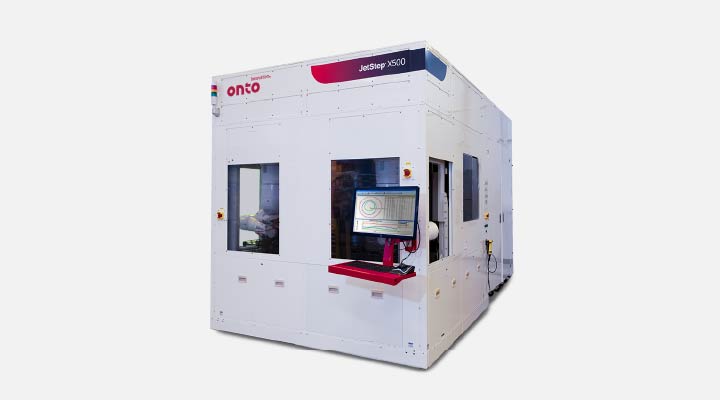
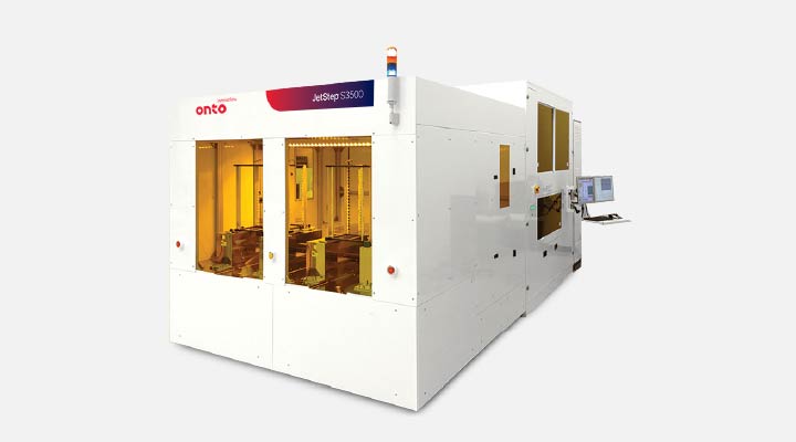
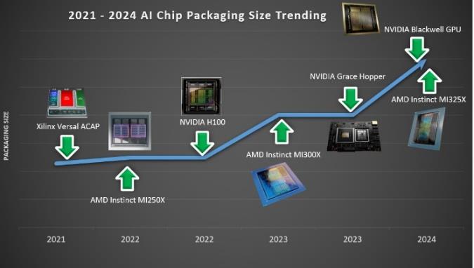
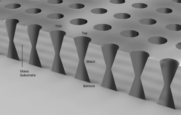
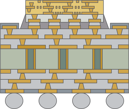
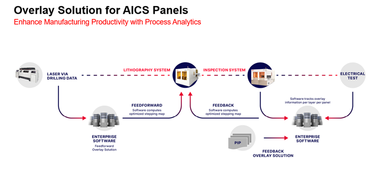
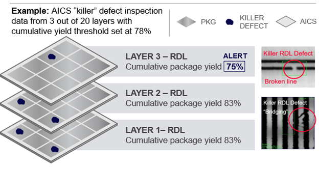
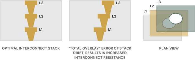
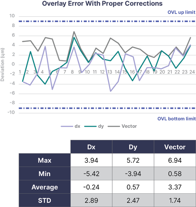
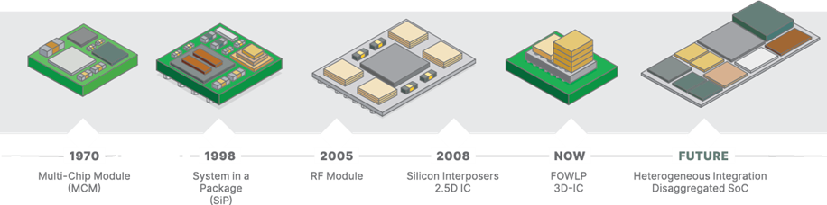
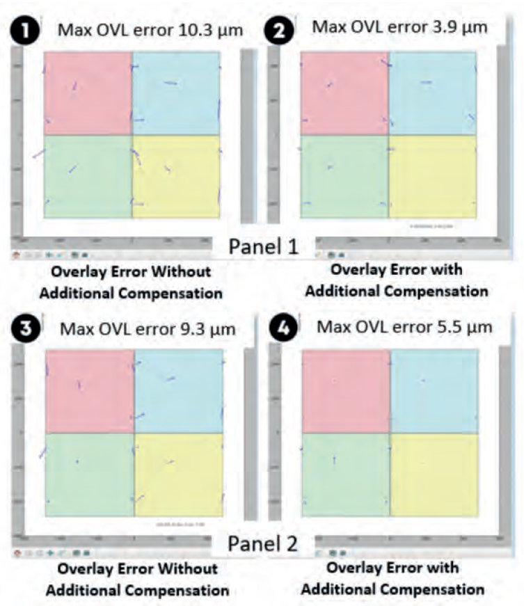
The future of AI technology is here, with new high performance computing designs and process architectures that support larger packages and require smaller, denser interconnects. As the advanced packaging roadmap evolves, the demand for larger package sizes grows, necessitating substrates that support high volume manufacturing. Enter, the panel. A panel substrate, whether organic or glass advanced IC substrates (AICS) or fan-out panel level packaging (FOPLP) with epoxy mold compound, offers approximately five times more area than a traditional 300mm wafer. High density interconnects are at the core of advanced packaging and high-resolution lithography at high throughput is essential to help the industry realize the advanced packaging roadmap. Our steppers are designed to tackle these manufacturing challenges, maximizing throughput while ensuring high resolution and precise overlay.

deco-bg-1 deco-bg-2
Related Products
View all
jetstepx500_feat

JetStep® X500 System

Designed for advanced integrated circuit substrates (AICS) and other advanced packaging manufacturing applications, incorporating a 250mm x 250mm large field exposure area achieving 3μm L/S resolution with a large depth of focus.
View Product
jetsetps3500_feat

JetStep® S3500 System

Advanced packaging lithography system designed for fan-out panel level packaging, accommodating substrates up to 720mm x 600mm
View Product
Related Insights & Resources
View all
Yield Prediction Technology

Yield Prediction Technology: A Game Changer for Cutting Costs and Reducing Ramp Time in FOPLP Lithography

Learn more
roadmap

The Innovations Driving the Advanced Packaging Roadmap, Part 1

Learn more
20240930_Onto_00461

Picking up the Pace of Panel-level Advanced Packaging at Onto Innovation

Learn more
the-long-climb

The Long Climb: Bringing Through Glass Vias (TGV) to High-Volume Manufacturing

Learn more
Overlay Optimization in Advanced IC Sub

Overlay Optimization In Advanced IC Substrates

Learn more
Picture1_240318_155910

How AI is Helping Optimize AI Chip Production

Learn more
glass-substrate_240212_181245

The Great Lithography Debate: Copper Clad Laminate or Glass Substrates?

Learn more
chip-sacle-review

Optimizing Advanced IC Substrates (AICS) for PLP

Learn more
Default product image

Total Overlay With Multiple RDLs with Keith Best

Learn more
glass-substrate

The Glass Substrate Question: When Will It Replace Copper Clad Laminate?

Learn more
overlay

Addressing Copper Clad Laminate Processing Distortion Using Overlay Corrections

Learn more
add-yield

Addressing Yield Challenges in Advanced IC Substrate (AICS) Packaging

Learn more
Address-image

Addressing Total Overlay Drift In Advanced IC Substrate (AICS) Packaging

Learn more
Correcting-Overlay

Heterogeneous Integration: Correcting Overlay Errors On Advanced Integrated Circuit Substrates (AICS)

Learn more
Het-Int

Heterogeneous Integration: Exposing Large Panels with Fewer Shots

Learn more
SC-Sept

‘XL’ Fine Resolution Large Field Lithography Dramatically Cuts FOPLP Pattern Distortion

Learn more
ECTC-2022-Image

Analysis of Pattern Distortion by Panel Deformation and Addressing it by Using Extremely Large Exposure Field Fine-Resolution Lithography

Learn more
fig-5_220126_110608

Outlier Control Technology and Feedforward Lithography Can Boost FOPLP Yield

Learn more
fine-res-litho

Large-field, Fine-resolution Lithography Enables Next-generation Panel-level Packaging

Learn more
Picture1_210722_090506

Advanced Outlier Die Control Technology in Fan-Out Panel Level Packaging Using Feedforward Lithography

Learn more
Extremely-large

Extremely Large Exposure Field With Fine Resolution Lithography Technology To Enable Next Generation Panel Level Advanced Packaging

Learn more
overlay-results

Adaptive Shot Technology To Address Severe Lithography Challenges For Advanced FOPLP

Learn more

Do you have a lithography question? Let’s talk!

As your partner for innovative solutions, we’re always here for you.

Discover how our cutting-edge semiconductor solutions are engineered to meet your most complex challenges: delivering performance, reliability and innovation where it matters most.

Let’s Talk

"*" indicates required fields

This field is for validation purposes and should be left unchanged.