Quick Search
Find a Product:
Product Categories
Worldwide Reach
Find Local Support:
Customer Success
Tech Trends
Corporate Responsiblity
Menu
Products & Technology
Customer Success
Insights & Resources
Company
Posted on Aug 26, 2025

Enabling In-Line Process Control for Hybrid Bonding Applications

As demand grows for high-performance computing (HPC) and AI-driven applications, manufacturers are turning to hybrid bonding to enable the ultra-dense 3D integration required for next-generation chip architectures.

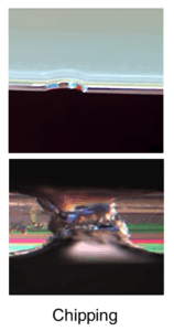
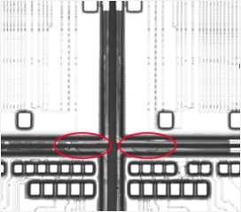
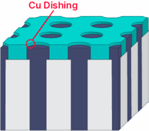
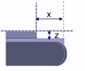
This advanced packaging technology presents significant process challenges. Surface preparation must be precisely controlled to eliminate particles, excess recess, and copper pad dishing, all of which can compromise bond quality. During pre-annealing, particle-induced gaps and wide bonding gaps can prevent proper wafer contact. Post-annealing, the formation of dielectric and metal voids introduces further risks to electrical performance and long-term reliability. If not carefully managed, these issues can lead to increased defectivity, reduced yield, and degraded performance in HPC and AI systems where reliability and speed are critical.
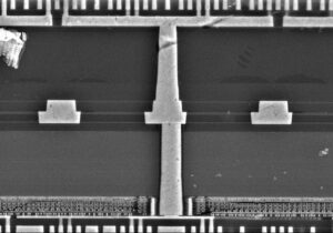
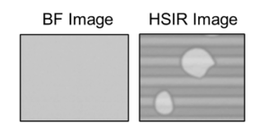
Hybrid bonding reliability starts with robust process control. Monitoring topography and detecting particles, cracks, and voids help identify defects early. Measuring copper pad dishing offers insight into surface conditions and planarity. Tight control during pre-bonding steps enables potential rework before permanent defects occur.

The following examples highlight key metrology and inspection techniques that support more consistent hybrid bonding outcomes.

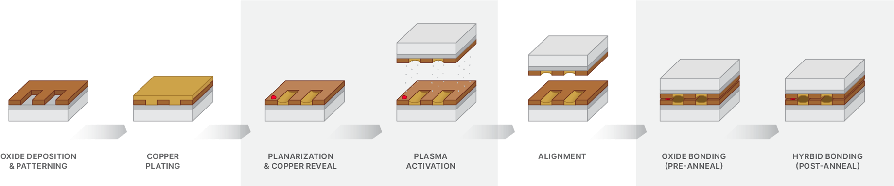
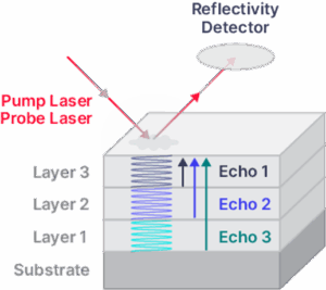
Pre-Bonding Process Control

deco-bg-1 deco-bg-2

Cu Seed/Barrier Thickness Measurements

As TSV becomes smaller, liner films become thinner.

Non-uniformity of liner deposition can result in liner under-coverage and device failure.

PULSE™ technology delivers high-accuracy, high-precision Cu seed/barrier thickness measurements, detecting deposition non-uniformities early. Its strong correlation to SEM/TEM enables reliable process optimization, helping ensure full liner coverage and reducing the risk of device failure.

Thin Film Measurement for CMP Top Layers

Multi-layer thin films are deposited to control post-CMP topography, and accurate measurement of pre- and post-CMP films is essential for effective CMP control.

High-precision pre- and post-CMP multi-layer stack measurement with dynamic repeatability for robust CMP process control.

Cu Recess Measurement

Accurate Cu recess measurement remains a key metrology challenge. Although atomic force microscopy (AFM) is commonly used in R&D for its precision, its low throughput and contamination risk limit its applicability in high-volume manufacturing.

Optical critical dimension (OCD) metrology offers a non-contact, high-throughput solution for Cu recess measurement, delivering high accuracy, precision, and strong correlation to AFM results—making it well-suited for high-volume manufacturing.

Edge Trim Metrology

Edge trimming is a critical process in wafer-to-wafer hybrid bonding, required to remove knife-shaped edges formed during wafer thinning. Without precise control, improper edge profiles can lead to chipping and delamination during wafer-to-wafer the bonding process.

Our long-range metrology sensor enables accurate step height measurement for edge trim profile characterization, capturing both depth (Z) and width (X) around the wafer edge. This non-contact solution provides the precision needed to monitor and control edge trim profiles, helping ensure reliability in hybrid bonding processes.

Particle Detection and Height Measurements

Surface particles pose a significant challenge in hybrid bonding, as they can lead to void formation at the bond interface. Characterizing these particles is essential for identifying defect sources and optimizing the bonding process to ensure yield and reliability.

Multiple integrated 3D metrology sensors enable precise particle height measurement, supporting either full-wafer inspection or sampling. This flexible capability provides critical data for wafer-to-wafer bonding quality and helps identify defect sources for process optimization.

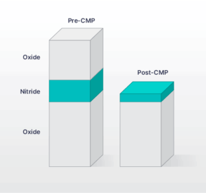
Post-Bonding Process Control

deco-bg-1 deco-bg-2

Pre/Post Anneal Void Detection

Void formation before and after annealing presents a critical reliability challenge. These voids can result from trapped gases, surface contamination, or insufficient bonding strength, impacting yield and long-term device performance.

The conventional process of record, C-SAM, faces several limitations, including poor sensitivity to micro-voids through full silicon thickness, edge inspection risks, and potential water leakage that can compromise sensitive wafer surfaces.

High speed IR enables 100% full wafer inspection at high throughput with flexible resolution and proven sensitivity down to voids as small as 2µm in dielectric layers.

Bonded Wafer Metrology and Inspection

Bonded wafer thickness uniformity directly influences the mechanical strength and structural integrity of the bonded stack during downstream processing. Variations in thickness and the presence of edge defects not only compromise bonding quality but also increase the risk of yield loss and reliability issues.

High-precision metrology for total and individual wafer thickness in multi-stacked bonded wafers, combined with automated edge inspection to detect defects and assess bonding quality, helps to ensure structural integrity and yield in hybrid bonding processes.

Die Crack Inspection

Die cracks can occur during the pick-and-place process in die-to-wafer (D2W) bonding and during final die sawing. Undetected cracks at any layer in a multi-die D2W stack compromise device reliability and yield, making early and accurate crack detection essential.

High speed infrared inspection enables inner die crack detection with 100% full wafer coverage at high throughput. Its flexible, multi-resolution imaging design helps to ensure reliable crack identification across all layers in the D2W process.