
Dragonfly® G5 System
The latest generation inline pattern inspection system in the Dragonfly series, delivering sub-micron defect detection and high resolution 3D metrology.

Specialty devices are the unsung heroes of modern life. For many in the semiconductor industry today, the spotlight is on the SiC and GaN power devices used in automotive, green energy, fast-charge consumer electronics (CE), and high-performance computing (HPC) applications.

May 5 — May 7, 2026
Onto Innovation is a proud exhibitor at SEMICON Southeast Asia.
The EB40 Module combines edge and backside inspection into one tool with the option to be paired with an inspection system to provide a high throughput all surface inspection solution.
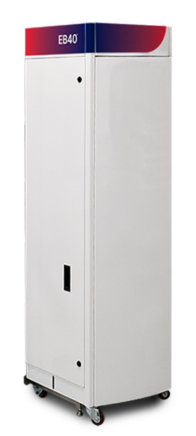
The Class 1 certified EB40 module offers combined edge and backside inspection and is also available as separate edge (E40) and backside (B40) modules. These modules provide brightfield and darkfield inspection to detect defects on the entire bevel and backside, covering Zone 1 to Zone 5. This enables faster root-cause analysis of defects that can migrate to the wafer interior, impacting die yield.
The EB40 module captures defect images on the fly, creates whole-wafer composite images, and integrates with SEM bevel review. All inspection and metrology results, including defect, whole wafer and SEM images can be analyzed together in a single database using Discover Defect software. Correlating EBR metrology with defectivity data, SEM data and micro-inspection results is just the beginning of what Discover software can do. In addition to advanced on-tool defect binning, real-time edge ADC classification can be assigned to defects prior to manual offline review using Discover Review software.


As your partner for innovative solutions, we’re always here for you.
Discover how our cutting-edge semiconductor solutions are engineered to meet your most complex challenges: delivering performance, reliability and innovation where it matters most.
"*" indicates required fields
The Dragonfly G3 system is resetting the industry’s expectations for throughput, accuracy and reliability. Combining 2D and 3D technologies, the system detects yield-robbing defects and measures features critical for today’s semiconductor technologies
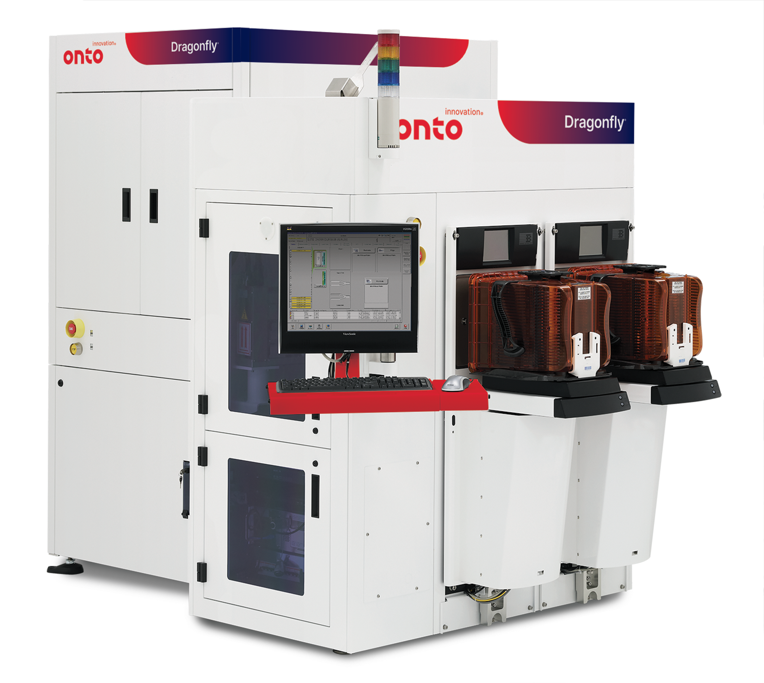
The Dragonfly G3 is a widely adopted pattern inspection system that utilizes line scan imaging technology to deliver fast, sub-micron defect detection for both R&D and high volume manufacturing environments. It features multiple illumination channels, including brightfield, darkfield, high-speed IR for embedded defects, and Clearfind® technology for detecting non-visual organic residues. Powered by modern machine learning algorithms, the Dragonfly G3 system offers a complete on-tool solution for defect detection, nuisance reduction and classification.
The system offers additional flexibility through the integration of multiple 3D metrology capabilities, including film thickness and structural profiling, and substrate thickness measurement. It features the latest 3Di™ technology, delivering and precise bump height metrology. The Dragonfly G3 system, with optional edge and backside inspection via the EB40 module, offers a comprehensive all-surface inspection solution for both front-end and back-end OQA.
Hybrid bonding enables ultra-dense 3D memory interconnects with up to 1,000x more connections than microbumps. Achieving high yield requires stringent process control, including monitoring topography and detecting particles, cracks and voids. Measuring dishing in copper pads provides valuable insight into surface conditions. Together, these process control insights contribute to improved device reliability and performance.

As demand grows for high-performance computing (HPC) and AI-driven applications, manufacturers are turning to hybrid bonding to enable the ultra-dense 3D integration required for next-generation chip architectures. This advanced packaging technology presents significant process challenges. Surface preparation must be precisely controlled to eliminate particles, excess recess, and copper pad dishing, all of which can compromise bond quality. During pre-annealing, particle-induced gaps and wide bonding gaps can prevent proper wafer contact. Post-annealing, the formation of dielectric and metal voids introduces further risks to electrical performance and long-term reliability.

The Iris S system is a versatile platform solution for the advanced packaging and specialty market, supporting 150mm, 200mm and 300mm wafers. It provides thin and thick film, OCD and wafer bow and film stress measurements.

The IMPULSE V system helps to advance CMP processing with enhanced wavefront technology and AI-driven analytics, delivering over 2X precision improvement and faster solutions, crucial for next-gen semiconductor manufacturing demands.
The Dragonfly G5 system is engineered for inline process control of leading-edge advanced packaging technologies. As the latest generation pattern inspection system in the Dragonfly series, it delivers unparalleled accuracy in detecting submicron defects and performing high-resolution 3D measurements.

The Aspect System is a revolutionary in-line, non-destructive infrared optical critical dimension (IRCD) system measuring Z-dimension profiling of high aspect ratio structures to enable critical process control. It meets the needs of leading-edge customers with its high speed and process coverage.


As your partner for innovative solutions, we’re always here for you.
Discover how our cutting-edge semiconductor solutions are engineered to meet your most complex challenges: delivering performance, reliability and innovation where it matters most.
"*" indicates required fields
The road to the future is not always a smooth, trouble-free drive. Along the way, there may be unforeseen detours, potholes and accidents, each one capable of setting progress back. But for those behind the wheel, those obstacles are just a part of the journey.
Such is the case for the automotive industry as it continues to steer away from gas-powered vehicles and turn toward hybrid and electric vehicles. To accomplish this, manufacturers of power devices are opting to use wide-bandwidth compound semiconductors like SiC and GaN. The reason: compound semiconductors accommodate higher voltages, faster switching speeds and lower losses than traditional silicon-based power devices.
For the purpose of our three-part series, we have been focusing on SiC power devices, the challenges presented by trench-based architectures that reduce on-resistance and increase carrier mobility, and the need to accurately measure epi layer growth and the depth of implant layers. Before we move onto the details of this blog, let’s take a quick look back at the previous two blogs.
You don’t have to be a dedicated follower of the transportation industry to know it is in the early stages of a significant transition, away from the rumbling internal combustion engine to the quiet days of electric vehicles. The signs of this transition are right there on the streets in the form of electric-powered buses, bikes and cars. The road to our electric future is before us, but we won’t be getting there without compound semiconductors like SiC.
Manufacturers in the automobile and clean energy sectors want more efficient power devices that can accommodate higher voltages, possess faster switching speeds and offer lower losses than traditional silicon-based power devices, something SiC power devices with trench structures can deliver.
But while trench-based architectures offer reduced on-resistance and increase carrier mobility, they bring along increased complexity. For manufacturers of SiC power devices, the ability to accurately measure epi layer growth and the depth of implant layers in these trenches is of considerable concern, especially when faced with ever-increasing fabrication complexity.
In the previous blog in this series, we explored how using an FTIR-based system allows for the direct modeling of carrier concentrations and film thickness, thus enabling SiC power device makers to better measure epi layer growth, implant layers and composition. In this installment, we explore how manufacturers of SiC power devices with trench-based structures measure trench depth and bottom and top critical dimension (CD) by using an optical critical dimension (OCD) metrology system designed for specialty devices.
The figures alone are impressive: SiC power devices are experiencing an annual average growth rate approaching 34% through 2027, according to the Yole Group. However, the potential for this amongst other compound semiconductor-based power devices such as gallium nitride (GaN) to change the world around us is even more impressive.
Thanks to the role that SiC-based devices play in the increased electrification of automobiles and the sustainable energy movement, the effort to make this world a cleaner, greener place is no longer a wished-for science fiction fantasy. It may one day be our reality. Perhaps even soon.
Manufacturers in the automobile and clean energy sectors want power devices that are more efficient and can accommodate higher voltages, faster switching speeds and lower losses than traditional silicon-based power devices. To accomplish this, they are turning to higher efficiency silicon carbide (SiC)-based devices.
When it comes to SiC power devices, most manufacturers have adopted a trench-based architecture. This reduces on-resistance and increases carrier mobility. However, these improvements come at the expense of rising fabrication complexity.
To address this issue, high-volume manufacturers of SiC power devices are, at several key steps, adopting inline process control methods, including optical metrology techniques like Fourier transform infrared (FTIR). With a system supporting FTIR optical metrology at their disposal, manufacturers can more accurately measure epi layer growth and the depth and accuracy of implanted dopants across the wafer, key challenges posed by the increased fabrication complexity of SiC power devices. In this blog, we’ll discuss how FTIR technology can help manufacturers successfully address these challenges.
Wind power. Rail. Solar energy. And, perhaps most significantly, electric and hybrid vehicles. Together, these four forces are among the major demand drivers for power devices.
While silicon (Si) still plays a role in power devices, wide-bandgap compound semiconductors like silicon carbide (SiC) and gallium nitride (GaN) are particularly well-suited for power devices thanks to their higher electron mobility, higher critical electric field and higher thermal conductivity. However, as new structures and larger wafer sizes become the norm for power devices, they bring with them distinct manufacturing challenges.
Today, the industry is transitioning from 150mm to 200mm wafers for SiC- and GaN-based devices and 200mm to 300mm wafers for Si-based devices. The reason: larger wafer sizes may help reduce the cost of fabrication. As the wafer size transition occurs, it is important to have a metrology tool that can measure a larger number of data points across the wafer without impacting the overall fab throughput. A loss of throughput adds to cost-of-ownership and may erase savings earned from transitioning to larger wafers.