


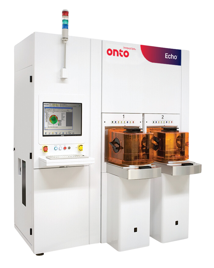
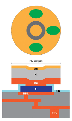
Echo™ System
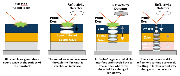
The Echo system utilizes picosecond ultrasonics to provide accurate, in-line, on-product metrology and materials characterization for semiconductor processes requiring metal thickness metrology, implant monitoring or thermal conductivity characterization on product wafers.
Product Overview
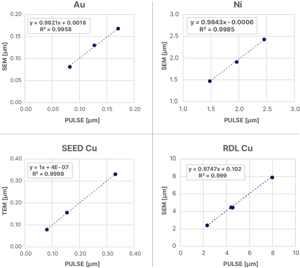
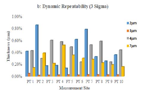
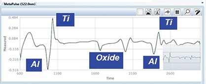
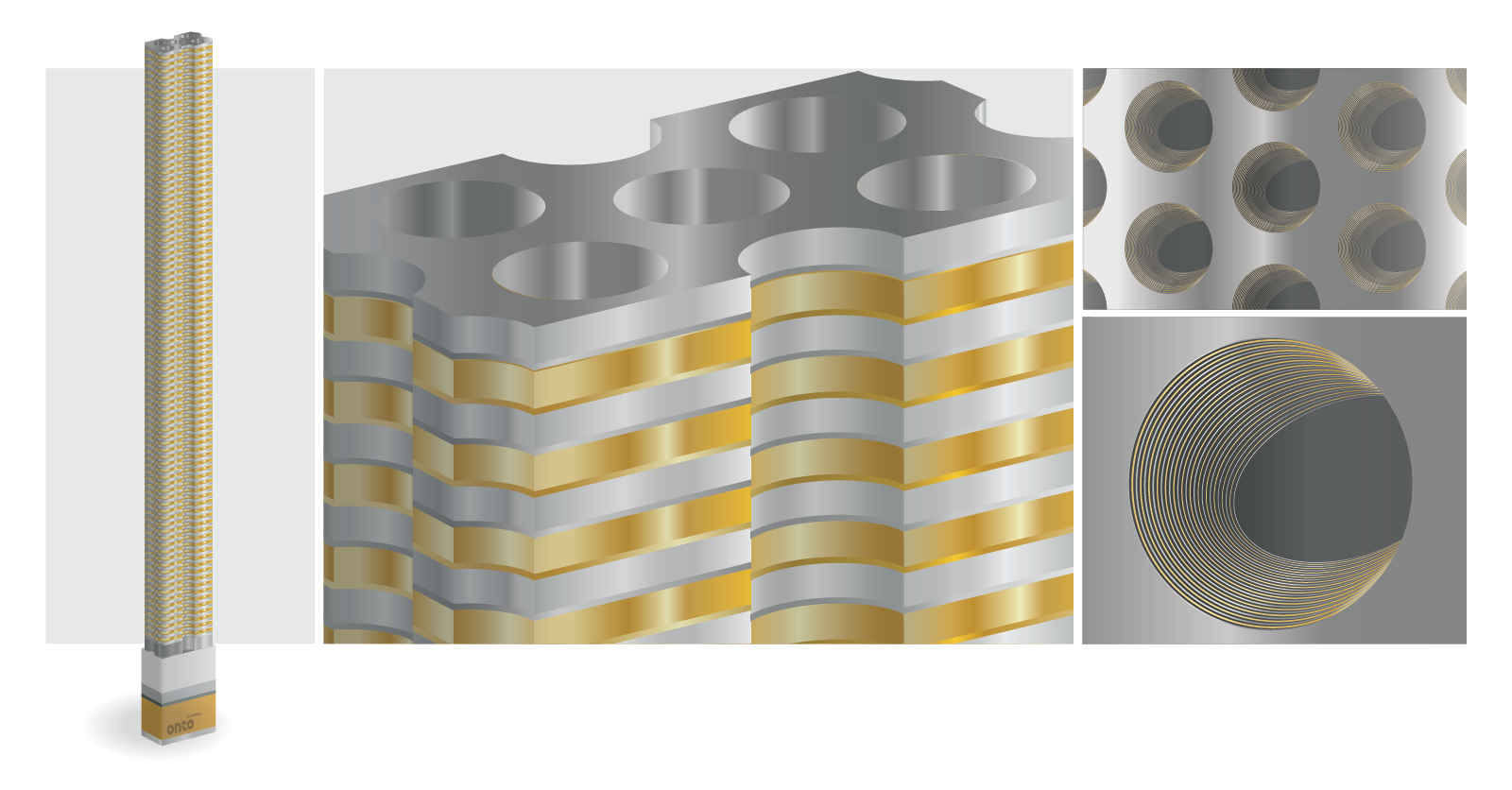
The Echo system is a comprehensive in-line metal film metrology tool designed for single and multi-layer metal film measurements in leading-edge logic, memory, advanced packaging and specialty semiconductor devices. Its innovative optics design extends the dynamic range for film thickness measurement from 50Å to 35µm on a single platform and offers extendibility to measure high aspect ratio advanced 3D NAND structures. The Expert Applications System (EASy™) software provides flexibility for developing user-defined algorithms to model complex multi-layer stacks.
The Echo system’s capabilities have been extended to include materials characterization. In addition to measuring the Young’s Modulus of low-k dielectric films in BEOL and amorphous carbon hard masks in 3D NAND, the Echo system includes proprietary electronics and algorithms for implant monitoring and thermal conductivity characterization. Its small spot size, combined with rapid measurements, enables full wafer mapping capabilities with 0.5mm edge exclusion, improving time to yield.
Applications
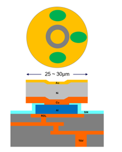
- Gate metals, plug/contact, barrier/seed layers, top metal
- RF electrode/IDT
- Advanced packaging UBM, RDL
- 3D NAND Hard mask
- MEMS Poly/Ge
- Low-k, ultra low-k film modulus, implant, thermal conductivity
Using Picosecond Ultrasonic Technology for AI Packages, Part 2
Front-End Technologies Are The New Back-End Tools: Using Picosecond Ultrasonics Technology For AI Packages, Part 1
Picosecond Ultrasonics: An Advanced Technology Utilized for Process Control of SiCr Thin Film Resistors
Advanced Interconnect Process Control with Picosecond Ultrasonic Technology for AI Device Packaging
Applications of Picosecond Laser Acoustics for Advanced Packaging
Using Picosecond Ultrasonics To Measure Trench Structures In SiC Power Devices

The Road to SiC Process Control
Optimizing Metal Film Measurement on IGBT And MOSFET Power Devices with Picosecond Ultrasonic Technology
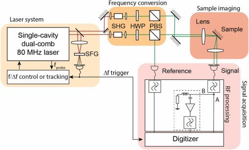
Efficient pump-probe sampling with a single-cavity dual-comb laser: Application in ultrafast photoacoustics
Paving the Way for 5G: RF Filter Process Monitoring and Control Using Picosecond Ultrasonic Metrology
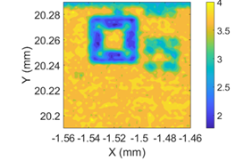
Imaging of Overlay and Alignment Markers Under Opaque Layers Using Picosecond Laser Acoustic Measurements
Advantages of Picosecond Ultrasonic Technology for Advanced RF Metrology
Full Metrology Solutions for Advanced RF with Picosecond Ultrasonic Metrology
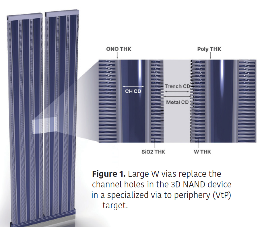
Monitoring Critical Process Steps in 3D NAND using Picosecond Ultrasonic Metrology with both Thickness and Sound Velocity Capabilities

Do you have an Echo system question? Let’s talk!
As your partner for innovative solutions, we’re always here for you.
Discover how our cutting-edge semiconductor solutions are engineered to meet your most complex challenges: delivering performance, reliability and innovation where it matters most.
Let’s Talk
"*" indicates required fields
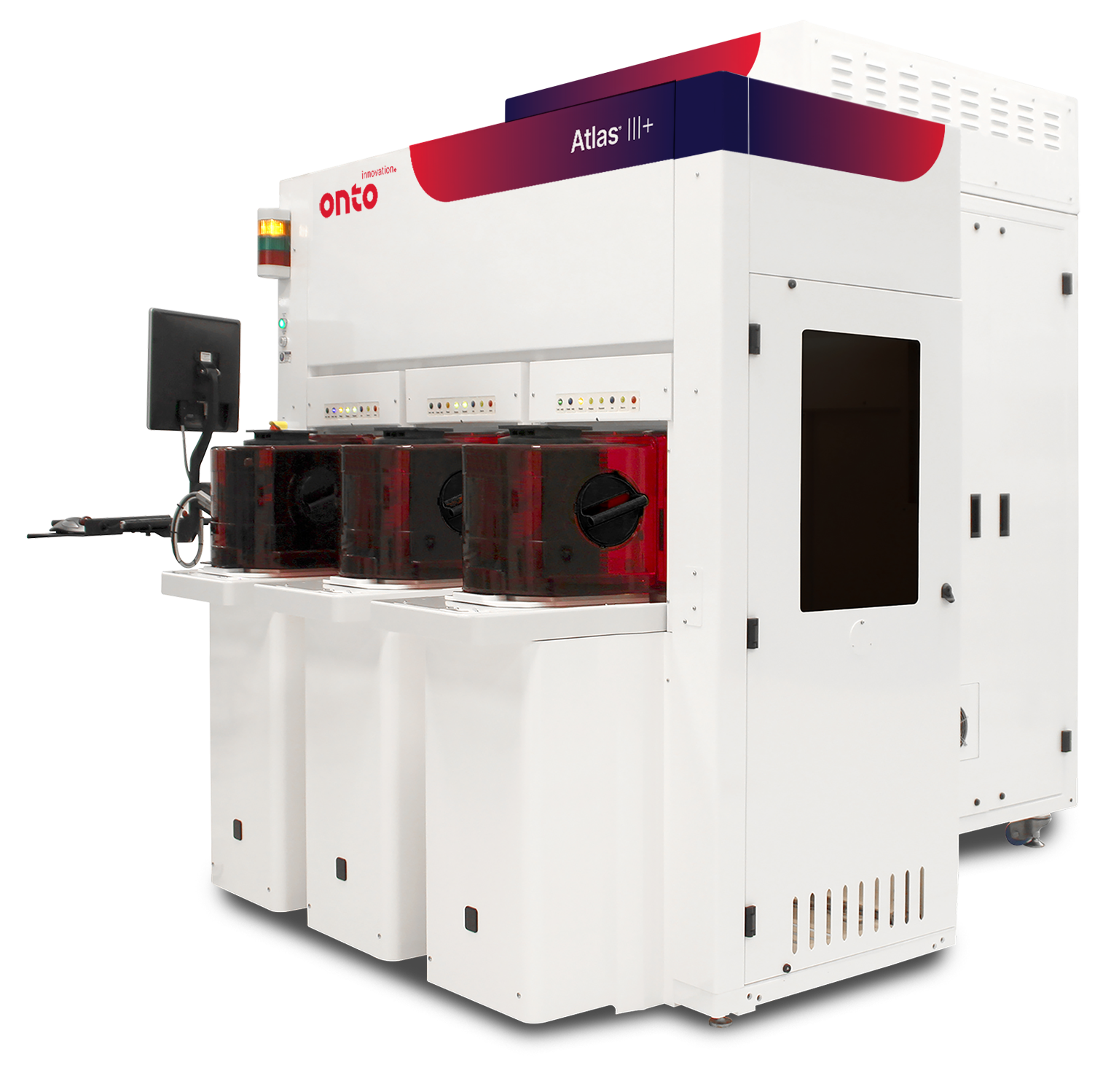
Atlas® III+ System
The Atlas III+ system provides dependable OCD and thin film metrology for established technologies, with flexible performance across a wide range of process layers and device types.
Product Overview
The Atlas III+ system is a widely adopted inline OCD metrology system, known for its robust and reliable solutions across all OCD and film layers from FEOL to BEOL. With its information-rich optical architecture, powerful OCD and machine learning analysis engine, the Atlas III+ system excels in advanced logic, 3D NAND and DRAM device processes. Extending metrology performance to sub-angstrom precision and accuracy levels, this system enables advanced process control across a broad range of applications in high volume manufacturing. The Atlas III+ system incorporates a proprietary spectroscopic reflectometry and spectroscopic ellipsometry solution, and when combined with Onto Innovation’s Ai Diffract™ OCD analysis software, it enables process control of every critical manufacturing unit operation. Users can gain insights into complex structure profiles across etch, clean, deposition and CMP steps.
Applications
- 3D-NAND
- DRAM: Logic and Foundry
- Specialty: CIS, AR/VR, Power & RF etc.
Intelligent Line Monitoring & Control with Integrated Metrology
Enhance CMP process control with a connected metrology approach that feeds forward data from standalone OCD or films metrology to integrated metrology, connected through AI-driven analytical software. This approach, powered by advanced modeling and analysis tools, can deliver high-precision, high-throughput results—minimizing or eliminating the need for and cost of new TEM data and enabling accelerated time to solution, faster excursion detection, reduced cost and improved Cpk.

Enhancing CMP Process Control with Intelligent Line Monitoring & Integrated Metrology
As semiconductor manufacturers push the boundaries of performance and functionality—driven by high-performance computing and AI applications—chemical mechanical planarization (CMP) processes increase in intensity complexity. New logic transistor designs, 3D NAND stacking, and DRAM integration introduce more CMP layers and tighter process windows.

IMPULSE® V System
The IMPULSE V system helps to advance CMP processing with enhanced wavefront technology and AI-driven analytics, delivering over 2X precision improvement and faster solutions, crucial for next-gen semiconductor manufacturing demands.

IMPULSE®+ System
The IMPULSE+ system is designed to deliver film measurement, fidelity and productivity in the CMP process module. Available as an integrated or standalone platform, it offers high sensitivity and accuracy.

Atlas® V System
The Atlas V system is an OCD and thin film metrology tool for high volume manufacturing, enabling FinFET & Gate-All-Around (GAA) logic, DRAM, and 3D NAND device process control.

Atlas® III+ System
The Atlas III+ system provides dependable OCD and thin film metrology for established technologies, with flexible performance across a wide range of process layers and device types.
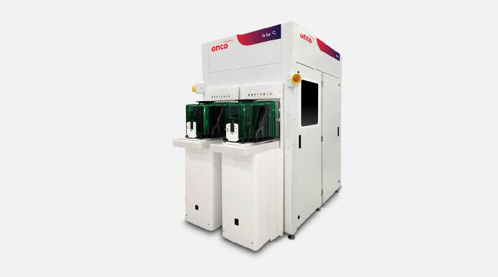
Iris™ S System
The Iris S system is a versatile platform solution for the advanced packaging and specialty market, supporting 150mm, 200mm and 300mm wafers. It provides thin and thick film, OCD and wafer bow and film stress measurements.
Iris™ G2 System
The Iris G2 system is an advanced optical metrology tool for both common and critical thin films for advanced node, mature and specialty devices, enabling manufacturers to increase transistor speed, reduce power consumption and improve reliability.

OCD Solutions
A suite of OCD modeling software and computing hardware that enables the full capability and connectivity across all Onto OCD and thin film metrology systems, including Atlas, Aspect, Iris and IMPULSE systems.
Atlas® G6 System
Leading edge OCD and thin film metrology for next-generation AI applications and beyond.
Atlas® V System
High performance OCD and thin film metrology for advanced GAA and memory devices.
IMPULSE® V System
Advanced high throughput integrated metrology system with AI-driven machine learning option. The system offers maximum sensitivity and accuracy to CMP process excursions and enables process engineers to establish APC control with high-accuracy feedback.
IMPULSE®+ System
Integrated metrology system offering maximum sensitivity and accuracy to CMP process excursions and enabling process engineers to establish APC control with high-accuracy feedback.

Aspect® System
Advanced infrared optical critical dimension (IRCD) metrology system for high aspect ratio structures in 3D NAND, 2D & 3D DRAM, CIS and power devices.
OCD Solutions
A suite of OCD modeling software and computing hardware offering comprehensive capabilities for inline metrology, offline recipe creation and fleet management.
Optical Critical Dimension Metrology for Semiconductor Manufacturing
Do you have an Atlas III+ system question? Let’s talk!
As your partner for innovative solutions, we’re always here for you.
Discover how our cutting-edge semiconductor solutions are engineered to meet your most complex challenges: delivering performance, reliability and innovation where it matters most.
Let’s Talk
"*" indicates required fields
Aspect® System
The Aspect System is a revolutionary in-line, non-destructive infrared optical critical dimension (IRCD) system measuring Z-dimension profiling of high aspect ratio structures to enable critical process control. It meets the needs of leading-edge customers with its high speed and process coverage.
Product Overview
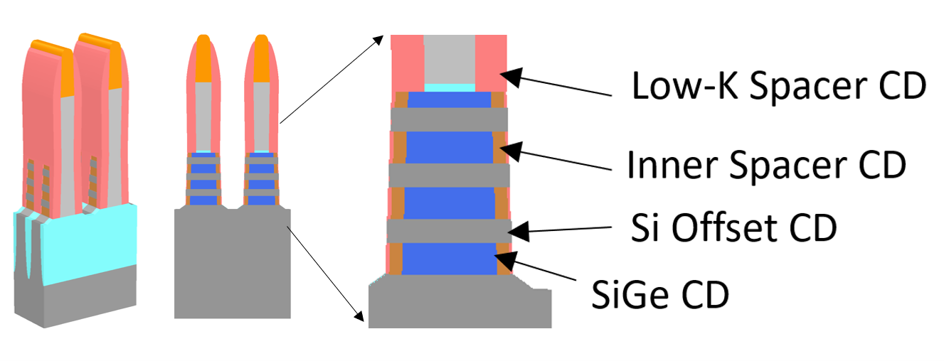
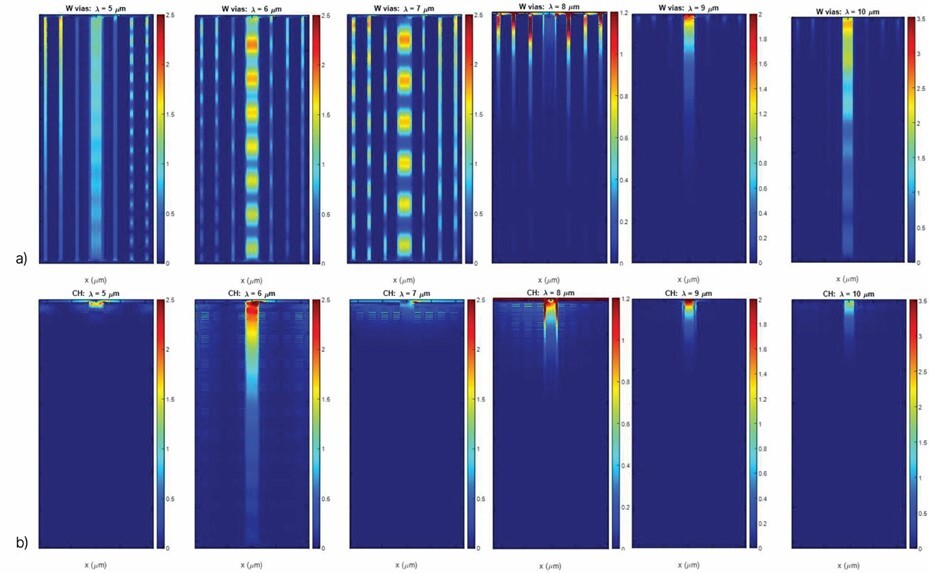
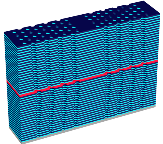
As the semiconductor industry relentlessly pursues density and power scaling, more and more high aspect ratio (HAR) processes are used across multiple device segments, especially in advanced memory such as 3D NAND and 3D DRAM. The Aspect metrology system was designed with these ongoing architectures and scaling strategies in mind. Aspect metrology has demonstrated superior performance across multiple customer devices through a unique proprietary IRCD system that provides full profiling capability to enable critical process control, with the speed and process coverage that customers require.
The Aspect system is powered by a software analysis engine, Ai Diffract™, that provides up to 90% faster time to solution which extends the industry leading NanoDiffract® software by leveraging extensive machine learning capabilities along with high fidelity modeling. The result is a simultaneous improvement in metrology performance along with a significant time to solution reduction.
Applications
- Etch, cleans, and deposition for 3D NAND
- Etch, cleans, and deposition for 2D and 3D DRAM
- Deep trench etch and doping for CIS
- Deep Trench etch in Power Devices
- On-device materials characterization for EPI process
Featured Markets
Hybrid Bonding Process Control Solution
Hybrid bonding enables ultra-dense 3D memory interconnects with up to 1,000x more connections than microbumps. Achieving high yield requires stringent process control, including monitoring topography and detecting particles, cracks and voids. Measuring dishing in copper pads provides valuable insight into surface conditions. Together, these process control insights contribute to improved device reliability and performance.

Enabling In-Line Process Control for Hybrid Bonding Applications
As demand grows for high-performance computing (HPC) and AI-driven applications, manufacturers are turning to hybrid bonding to enable the ultra-dense 3D integration required for next-generation chip architectures. This advanced packaging technology presents significant process challenges. Surface preparation must be precisely controlled to eliminate particles, excess recess, and copper pad dishing, all of which can compromise bond quality. During pre-annealing, particle-induced gaps and wide bonding gaps can prevent proper wafer contact. Post-annealing, the formation of dielectric and metal voids introduces further risks to electrical performance and long-term reliability.

Iris™ S System
The Iris S system is a versatile platform solution for the advanced packaging and specialty market, supporting 150mm, 200mm and 300mm wafers. It provides thin and thick film, OCD and wafer bow and film stress measurements.
IMPULSE® V System
The IMPULSE V system helps to advance CMP processing with enhanced wavefront technology and AI-driven analytics, delivering over 2X precision improvement and faster solutions, crucial for next-gen semiconductor manufacturing demands.

Dragonfly® G5 System
The Dragonfly G5 system is engineered for inline process control of leading-edge advanced packaging technologies. As the latest generation pattern inspection system in the Dragonfly series, it delivers unparalleled accuracy in detecting submicron defects and performing high-resolution 3D measurements.
Aspect® System
The Aspect System is a revolutionary in-line, non-destructive infrared optical critical dimension (IRCD) system measuring Z-dimension profiling of high aspect ratio structures to enable critical process control. It meets the needs of leading-edge customers with its high speed and process coverage.
Atlas® V System
High performance OCD and thin film metrology for advanced GAA and memory devices.
Atlas® III+ System
Versatile OCD and thin film metrology for mature and mainstream nodes.
Element™ S System
Transmission and reflection combined FTIR Measurement for wafer, specialty devices, supporting 100-200mm wafer sizes.
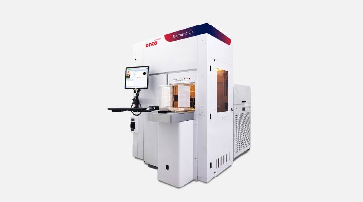
Element™ G2 System
Transmission and reflection combined FTIR measurement for advanced epi thickness, film composition control and advanced IR modeling.
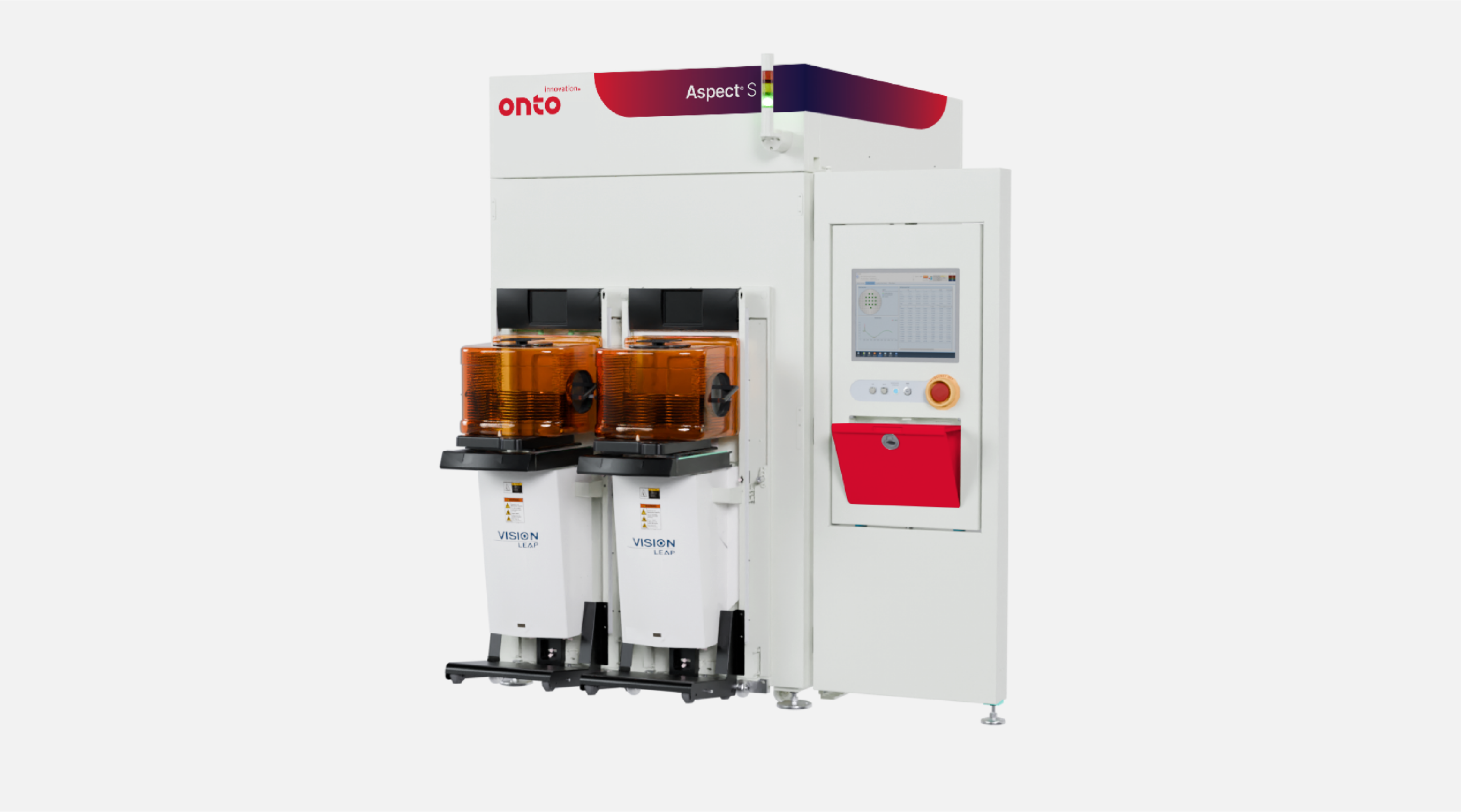
Aspect S System
Advanced model-based infrared reflectometry (MBIR) metrology system for in-line monitoring of 3D structures used in V-NAND, CIS and power devices, as well as carbon hardmasks, dielectric compositions and epitaxial layer stacks.
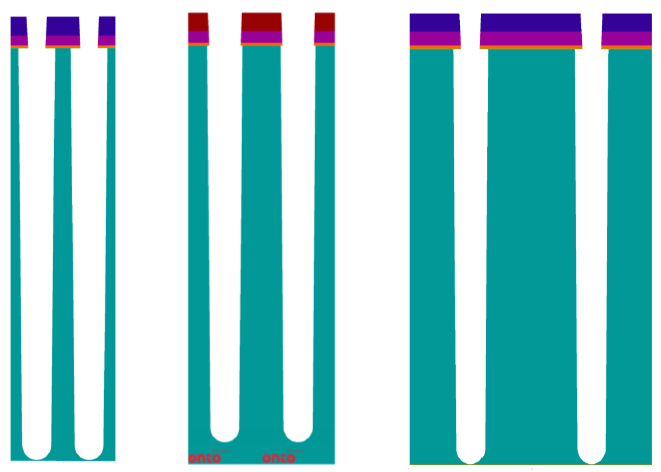
Non-destructive Measurement of Bottom Width in Deep Trench Isolation Structures Using IRCD Metrology
3D NAND Needs 3D Metrology
Measuring the Critical W-recess in 3D NAND
Critical Moves: Advanced Logic Devices And CIS Benefit From Applications Using IRCD Metrology
Mid-Infrared Optical Metrology for High Aspect Ratio Holes in 3D NAND Memory Manufacturing
Untangling 3D NAND: Tilt, Registration, and Misalignment
Do you have an Aspect system question? Let’s talk!
As your partner for innovative solutions, we’re always here for you.
Discover how our cutting-edge semiconductor solutions are engineered to meet your most complex challenges: delivering performance, reliability and innovation where it matters most.
Let’s Talk
"*" indicates required fields
NSX® 330 System
The NSX 330 system offers advanced macro inspection for a wide range of defect sizes at high throughput, with optional 3D metrology integration.
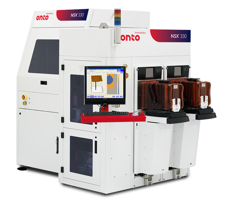
Product Overview
The NSX 330 system features robust platform technology with high-acceleration staging, high-speed multi-processor computing and flexible software. With over 1,000 installation worldwide, the NSX 330 System offers 2D inspection and metrology at high throughput and a broad portfolio of 3D sensors supporting critical advanced packaging applications. These include wafer-level metrology for micro bumps, RDL, kerf, overlay, and through silicon via (TSV) in a single wafer load.
Accommodating wafers from 100mm to 330mm, the system features a versatile objective turret, programmable light tower, and multiple dark field illumination modes. Additional features include resolution flexibility, unique handling solutions, and comprehensive software for recipe sharing and offline analysis. The NSX 330 system, with optional edge and backside inspection via the EB40 module, provides a comprehensive all-surface inspection solution packaging technology challenges.
Applications
- Macro inspection: whole wafer, and film frame
- Gel and waffle pack inspection
- OQA and post saw
- Post Probe and Testing
- Substrate thickness, TTV, and bonded wafer thickness stack thickness (carrier, adhesive, product wafer and total stack)
- Via depth thick and thin RST
- Bow and warp
Featured Markets

Dragonfly® G3 System
Highly configurable, automated, high speed 2D inspection and 3D metrology for inline process control in advanced packaging, specialty and front-end OQA.

EB40™ Module
Edge and backside inspection.

Discover® Defect Software
Integrated defect management system that works seamlessly with Onto tools and your entire enterprise, bringing data together for greater visibility and cleaner operation.

Discover® Review Software
Your smart factory’s human classification interface.
Understanding Optical Inspection For CIS
Do you have an NSX 330 system question? Let’s talk!
As your partner for innovative solutions, we’re always here for you.
Discover how our cutting-edge semiconductor solutions are engineered to meet your most complex challenges: delivering performance, reliability and innovation where it matters most.
Let’s Talk
"*" indicates required fields
F30™ System
The F30 system is designed to blur the lines between dark field micro inspection and traditional macro inspection, providing automated defect inspection for front-end and outgoing quality (OQA) applications.
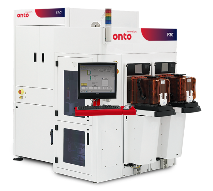
Product Overview
The F30 automated defect inspection system combines high resolution and throughput to drive fab yield and productivity. A five-objective turret enables resolution-throughput flexibility, while its multi-channel illumination including brightfield, darkfield, high-angle ring light, and IR-Review addresses the requirements for today’s multi-process inspection applications. Equipped with an advanced productivity suite (waferless recipe creation, simultaneous FOUP, recipe server and tool matching), the F30 System redefines inspection cost of ownership expectations. The system can handle 100mm – 300mm wafers can be paired with the edge and backside module (EB40) to provide an all-surface inspection solution.
Applications
- After develop inspection (ADI)
- Post CMP inspection
- After etch inspection
- Fab Outgoing QA
Featured Markets
Discover® Defect Software
Integrated defect management system that works seamlessly with Onto tools and your entire enterprise, bringing data together for greater visibility and cleaner operation.
EB40™ Module
Edge and backside inspection.

TrueADC® Software
Automated defect classification software with deep learning, real defect modeling and seamless integration with Onto AOI tools.
Do you have a F30 system question? Let’s talk!
As your partner for innovative solutions, we’re always here for you.
Discover how our cutting-edge semiconductor solutions are engineered to meet your most complex challenges: delivering performance, reliability and innovation where it matters most.
Let’s Talk
"*" indicates required fields
Celero™ PL System
The Celero PL system is designed for subsurface defect inspection and classification for silicon carbide (SiC) and gallium nitride (GaN) based wafers and compound semiconductor materials.
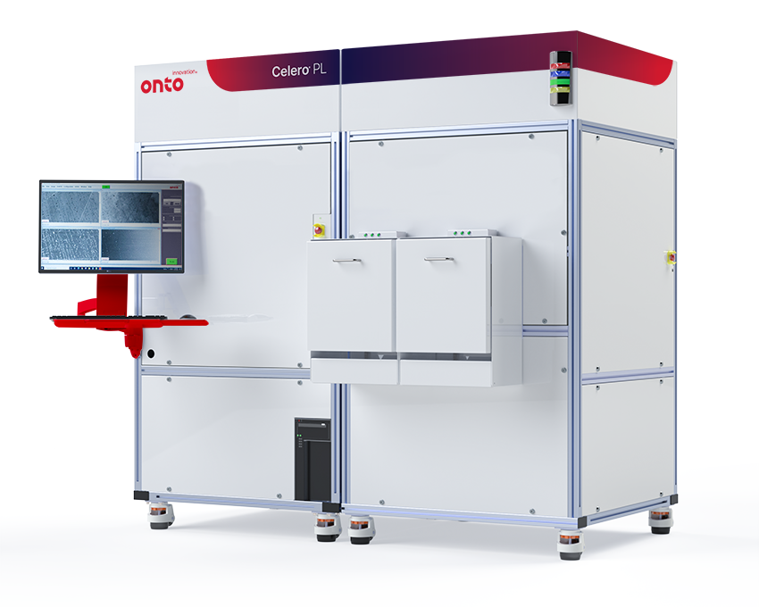
Product Overview
The Celero PL system utilizes a laser-based phase detection and imaging capability that leverages custom optics and image processing algorithms to enable best in class throughput and sensitivity for silicon carbide and gallium nitride-based materials on 100mm to 300mm wafer sizes. Leveraging multiple light sources and sensor channels, the system can detect, measure and image a broad variety of subsurface crystalline defects, associated with bulk wafers and epitaxial layers, surface particles, scratches, pits, surface contamination, stains, point or bulk wafer stress, voids/inclusions, including chips and cracks at the edge of the wafer.
Applications
- Frontside / backside / edge / subsurface defectivity and contamination
- Crystalline defectivity in III-V substrates and epitaxial layers
- Thick wafer / seed wafer surface and sub-surface defectivity
- Substrate-to-epitaxial layer defect mapping (sub-defect mapping)
- Wafer based microLED / VCSEL / EE laser materials
Featured Markets

PrimaScan™ System
All-surface defect and contamination inspection for unpatterned wafer and blanket films, with imaging capability for opaque, transparent and semi-transparent wafers, reticles and piece parts.

PrimaScan™ R&D System
All-surface defect and contamination inspection for unpatterned wafer and blanket films, with imaging capability for opaque, transparent and semi-transparent wafers, reticles and piece parts.
Do you have a Celero PL system question? Let’s talk!
As your partner for innovative solutions, we’re always here for you.
Discover how our cutting-edge semiconductor solutions are engineered to meet your most complex challenges: delivering performance, reliability and innovation where it matters most.
Let’s Talk
"*" indicates required fields