
Discover® Defect Software
Integrated defect management system that works seamlessly with Onto tools and your entire enterprise, bringing data together for greater visibility and cleaner operation.
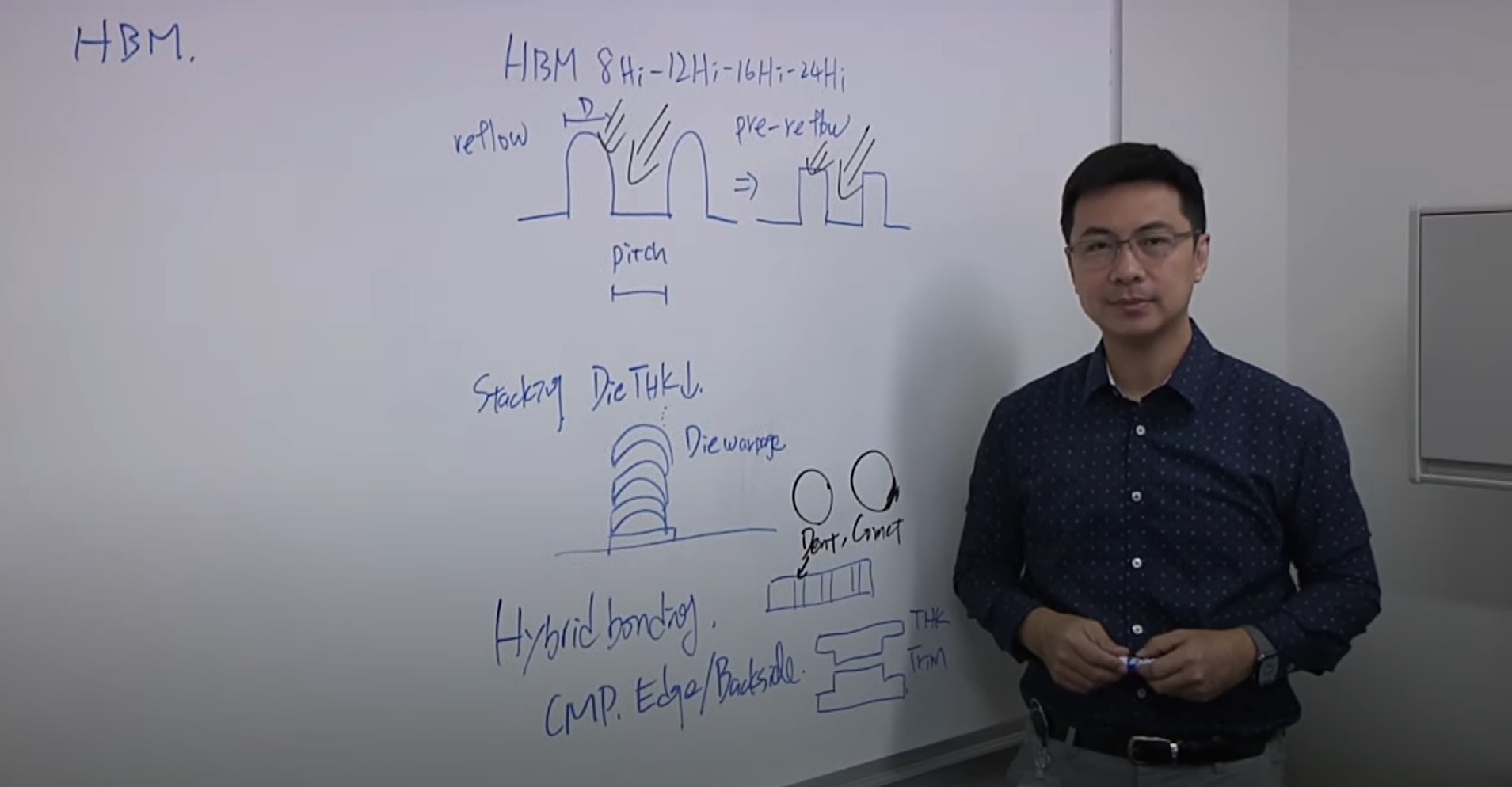
Learn how to reduce stress that causes warpage, how HBM architectures will need to change, and what happens when hybrid bonding and co-packaged optics are added into these devices from Onto Innovation's topical video with Semiconductor Engineering.

Nov 18 — Nov 21, 2025
Onto Innovation is a proud exhibitor at SEMICON Europa!
Yield Optimizer software is part of a comprehensive next-level data management portfolio. It reimagines manufacturing line control and analytics to explore the impact of previously invisible factors in day-to-day factory operation.
Yield Optimizer software is the next incarnation of analytics on the evolutionary scale. The software’s disruptive technology analyzes relationships between multivariant data and their complex interactions. By examining any set of conceivable inputs and outputs, Yield Optimizer software identifies the relationships and interactions that lead to positive operational changes. Easily understood visuals empower even casual users to understand what is important before making adjustments.
Yield Optimizer software evaluates multiple models and suggests the best one for the data. Using machine learning, it examines the interactions between in-process metrology readings and end-of-line test results for any semiconductor product family and recommends changes to the in-process metrology targets. When licensed as a service, it enables users to leverage an on-demand infrastructure to apply easily understood workflows for complex analytics without the overhead.
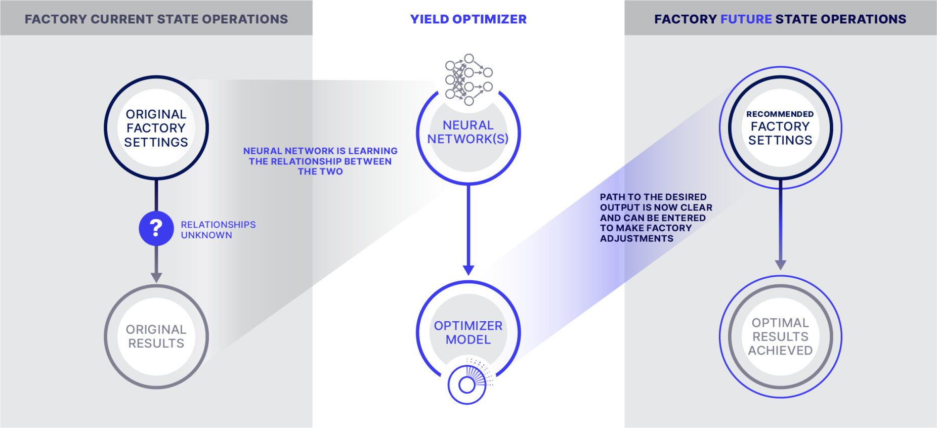
Neural networks model today’s data to achieve tomorrow’s in-line targets
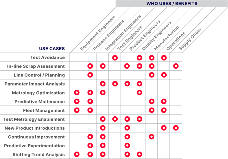
Users across the fab benefit from Yield Optimizer software’s easy-to-apply analytics


As your partner for innovative solutions, we’re always here for you.
Discover how our cutting-edge semiconductor solutions are engineered to meet your most complex challenges: delivering performance, reliability and innovation where it matters most.
"*" indicates required fields
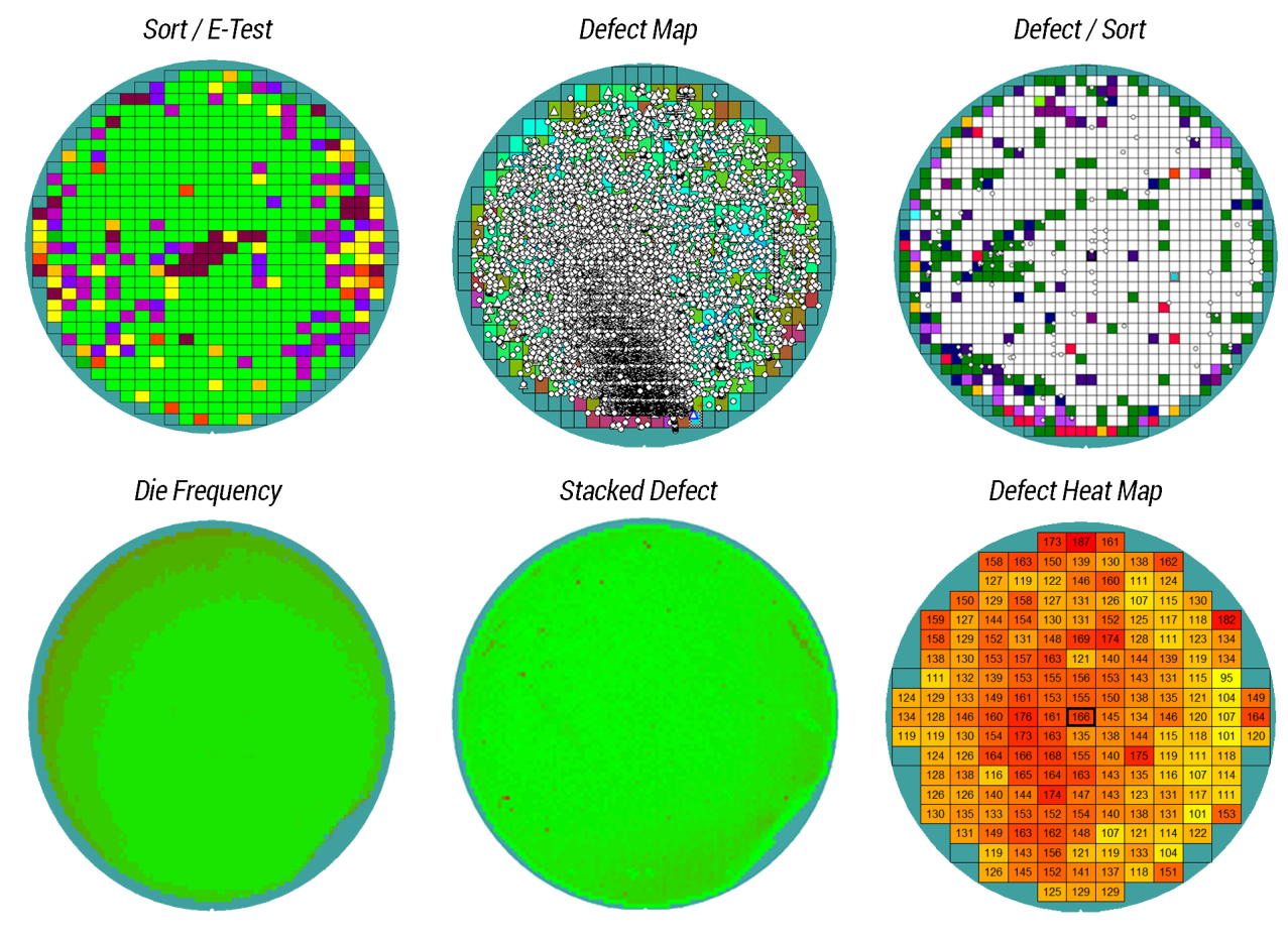
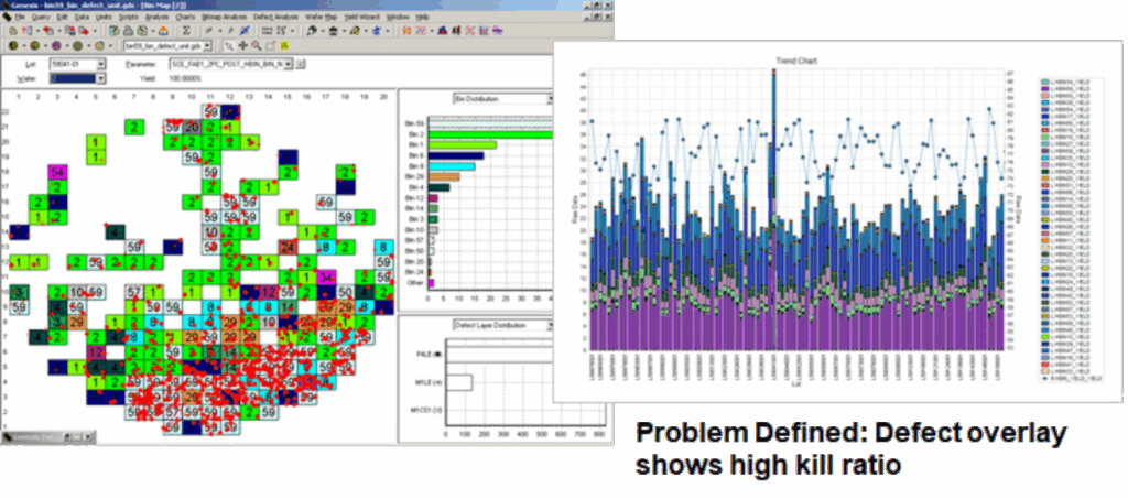
Discover Defect software provides actionable value to raw data through its intelligent, real-time analytics techniques. Inline monitoring, alarming and reporting is standard with all inspection tools, as well as offline fab-wide analysis with all licensed third-party tools.
Discover Defect software readily integrates into any wafer or panel production environment. It flexibly brings together all pertinent fab information, including defect, sort, metrology, wip, and electrical, into a single big data-capable solution. Its speed and up-time are world class.
Discover Defect software will pay for itself repeatedly by enabling its users to identify and solve problems, as well as to monitor and alarm on known areas of concern quickly and accurately. The product is designed to improve both throughput and yield while simultaneously reducing manufacturing costs.
Expand your yield analysis capabilities with the power of the Discover Yield software module. Discover Yield software’s patented data mining capabilities and advanced statistical analysis allow for highly sophisticated, interactive root cause analysis. Discover Yield software gives you the power to deep-dive into your data to uncover even the most difficult-to-identify systemic process issues.
Comprehensive mapping suite that covers all aspects of semiconductor processes
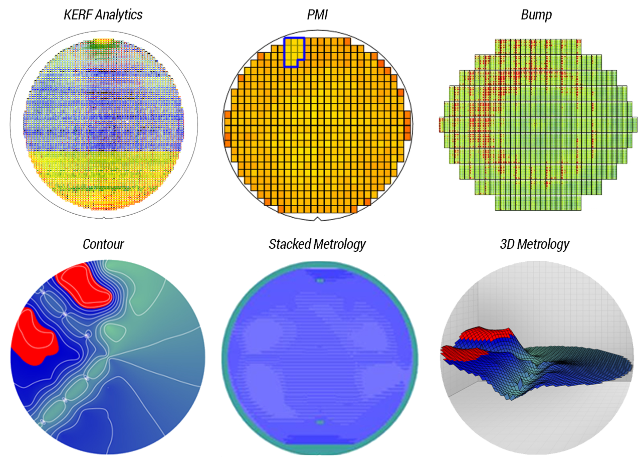
Targeted modules specific to customer challenges


As your partner for innovative solutions, we’re always here for you.
Discover how our cutting-edge semiconductor solutions are engineered to meet your most complex challenges: delivering performance, reliability and innovation where it matters most.
"*" indicates required fields
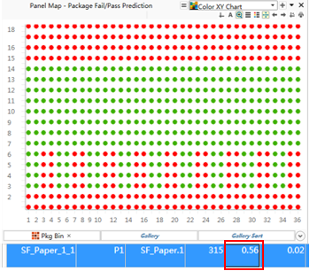
Discover Yield software is a complete yield management enterprise platform that combines parametric, defect and yield optimization with data mining and workflow development across all data sources from memory and design to assembly and packaging.
Discover Yield software helps reduce the time it takes to find root causes of yield excursions and enables manufacturers to broaden their analysis scope for better yield management.
The software includes data acquisition and integration, a development environment through workflow and scripting, and specialized analysis algorithms to identify domain-specific issues, such as data mining, spatial anomalies, wafer processing sequence problems, commonality of effects, system and random yield loss, chamber matching, tool events, traceability and more. In addition, Discover Yield software provides distinct tools – principal components and multivariate analysis of variance (MANOVA) – that allow systematic, simultaneous examination of multiple variables. Discover Yield software’s database architecture for genealogy uniquely supports value chain predictive analytics.
Improving baseline yield with analytics


As your partner for innovative solutions, we’re always here for you.
Discover how our cutting-edge semiconductor solutions are engineered to meet your most complex challenges: delivering performance, reliability and innovation where it matters most.
"*" indicates required fields
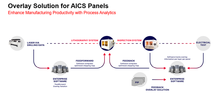
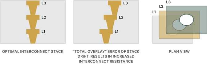
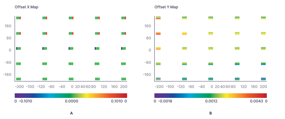
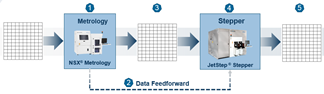
An advanced feed-forward lithography software solution for fan-out panel level packaging that enhances yield and throughput by correcting die placement errors through external measurements, predictive analytics and adaptive shot control.
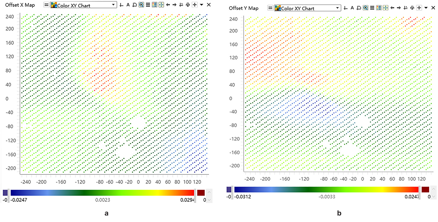
StepFAST® software is Onto Innovation’s advanced lithography software solution tailored for fan-out panel-level packaging, where die placement errors and material instability can significantly impact yield and productivity. StepFAST® software uses a feed-forward adaptive shot approach, integrating high-speed die placement measurements from the Firefly® system and applying real-time corrections to every shot of the JetStep® lithography tool. This external measurement strategy doubles throughput compared to traditional on-tool (self-metrology) methods. The software also incorporates predictive yield analysis, enabling dynamic adjustment of exposure field sizes to balance throughput and overlay accuracy. By automating reticle selection and optimizing field coverage, StepFAST® software ensures efficient panel exposure while minimizing registration errors—from ±50µm down to under ±3µm. With advanced analytics, StepFAST® software transforms lithography into a flexible, high-efficiency process, delivering substantial improvements in yield, throughput, and cost of ownership for panel-level packaging applications.
Die shift on reconstituted panels can significantly impact both productivity and yield. To address this challenge, we use a parallel die placement measurement process and advanced analytics to provide a means to balance productivity against yield. Our integrated lithography cell, featuring Firefly inspection, StepFAST software, and JetStep Lithography, delivers industry-leading throughput and yield for fan-out panel level packaging.
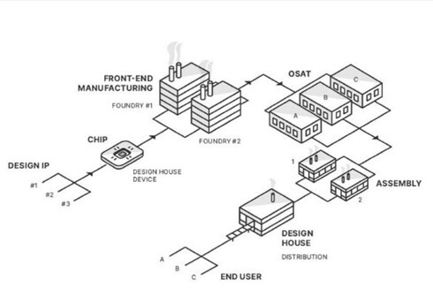
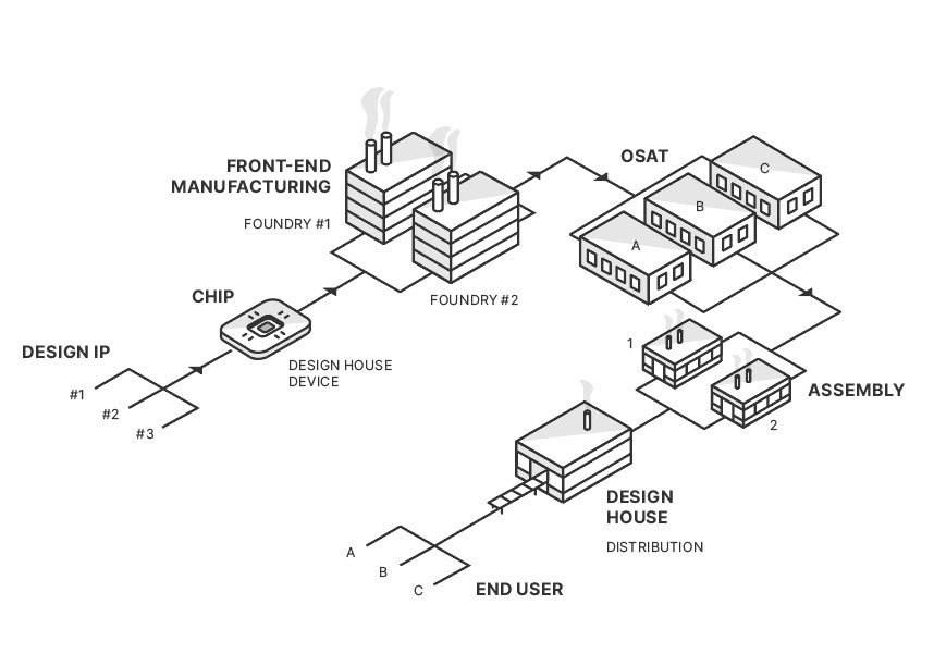
It is well understood that advanced packaging applications require high performance, low cost, increased functionality and improved reliability that 2.5D and 3D packaging solutions provide. Fan-out panel-level packaging (FOPLP) is one of the technologies that has the potential to meet these packaging requirements.
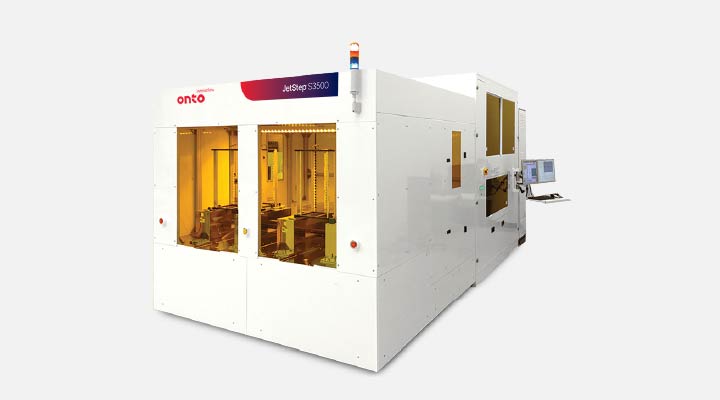
The JetStep S3500 system is designed to provide OSATS with a high-volume manufacturing advanced packaging lithography solution. For substrates up to 720mm x 600mm, it supports fan-out panel level packaging.
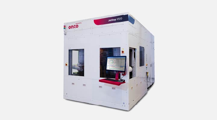
The JetStep X500 system is designed to provide AICS and OSAT manufacturers with a high-volume manufacturing lithography solution for heterogeneous integration. The JetStep X500 system exposes panel-type substrates made of CCL, FR4, composite, glass or other materials.
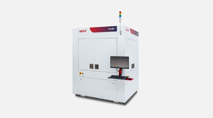
The Firefly G3 system provides automated inspection and 3D metrology for advanced IC substrates and panel level packaging, delivering high resolution and productivity for demanding applications like high-performance computing (HPC), artificial intelligence (AI), cloud computing and machine/deep learning.

An advanced feed-forward lithography software solution for fan-out panel level packaging that enhances yield and throughput by correcting die placement errors through external measurements, predictive analytics and adaptive shot control.
As your partner for innovative solutions, we’re always here for you.
Discover how our cutting-edge semiconductor solutions are engineered to meet your most complex challenges: delivering performance, reliability and innovation where it matters most.
"*" indicates required fields
The IVS 280 system delivers overlay, CD and z-height metrology for 100mm-200mm wafers. It is designed to meet the challenging requirements of power, compound semi and MEMS segments.
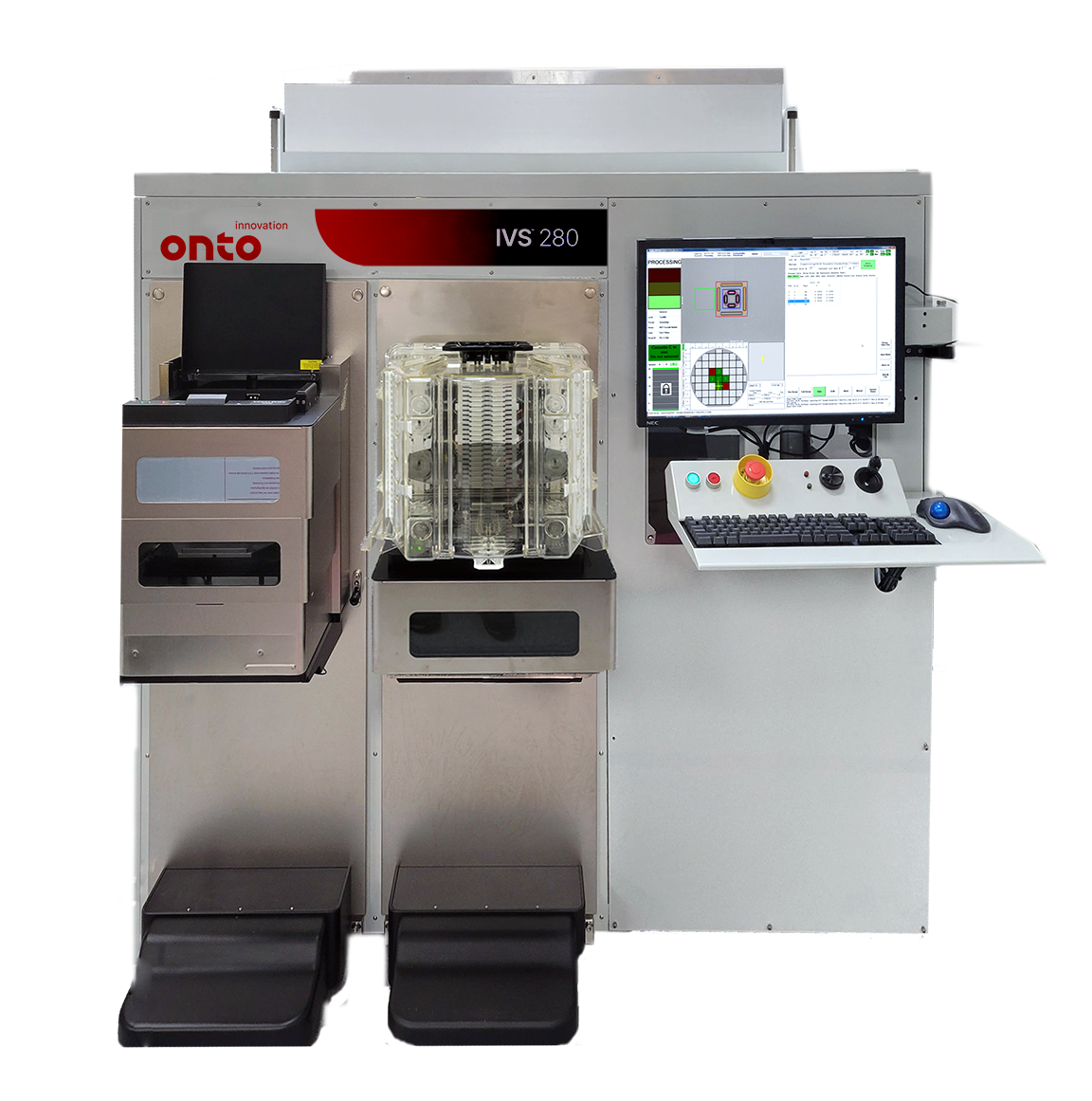
The IVS 280 system has been designed for ultimate precision, tool induced shift (TIS) and throughput for 100mm to 200mm wafers, with a mean time between failure (MTBF) > 2,000 hours. The IVS 280 system provides the same capability in a system designed for overhead track handling with full capability per SEMI® standards.
Flexibility is key in compound semiconductor processes, accommodating various wafer sizes, thicknesses, and compositions, including versatile wafer handling for Si, SiC, quartz, glass, GaAs, GaN, and LiNO3 wafers.
Its robust wafer handling and navigation system requires no operator assistance during recipe execution. The IVS 280 system enables wafer size changes without hardware alterations. Recipes and data remain stable over time. The system also supports recipe transfers from older IVS platforms like the IVS 200 and IVS 220.
The demonstrated capabilities of the IVS system to perform with high precision and solid reliability set this system apart.
Enter your information below and we’ll send you a unique passcode to view our IVS 3D Demo.
As your partner for innovative solutions, we’re always here for you.
Discover how our cutting-edge semiconductor solutions are engineered to meet your most complex challenges: delivering performance, reliability and innovation where it matters most.
"*" indicates required fields
The Iris S system is a versatile platform solution for the advanced packaging and specialty market, supporting 150mm, 200mm and 300mm wafers. It provides thin and thick film, OCD and wafer bow and film stress measurements.
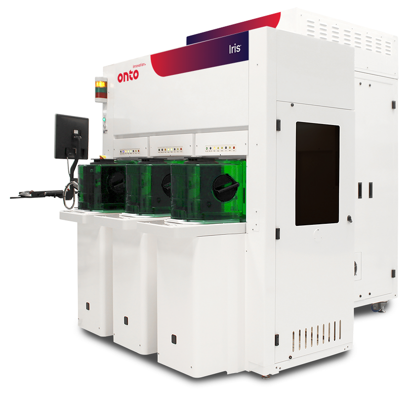
The Iris S system delivers films metrology and advanced OCD capabilities for the specialty and advanced packaging segments. With a small footprint, it handles 150mm, 200mm, and 300mm wafer sizes, including thin, thick and bonded wafers. The system supports various materials such as Si, SiC, GaN and glass, addressing device-level challenges impacting performance and yield. Leveraging Onto’s Ai Diffract™ software, the Iris S system supports the most difficult on-wafer high value problems.
The Iris S system includes a dual-arm robot, high-precision stage, advanced pattern recognition, and high-speed focus for accurate positioning at high throughput. The dual channel optical architecture offers oblique incidence Mueller Matrix spectroscopic ellipsometry (MMSE) and normal incidence spectroscopic reflectometry (SR) in a broad wavelength range from UV to IR.
Based on Windows 10 OS and a 64-bit architecture, the Ai Diffract™ software interface and automation comply with SEMI standards. Onto’s model guided machine learning enables fast, flexible and robust film and OCD recipe setup.
Enhance CMP process control with a connected metrology approach that feeds forward data from standalone OCD or films metrology to integrated metrology, connected through AI-driven analytical software. This approach, powered by advanced modeling and analysis tools, can deliver high-precision, high-throughput results—minimizing or eliminating the need for and cost of new TEM data and enabling accelerated time to solution, faster excursion detection, reduced cost and improved Cpk.

As semiconductor manufacturers push the boundaries of performance and functionality—driven by high-performance computing and AI applications—chemical mechanical planarization (CMP) processes increase in intensity complexity. New logic transistor designs, 3D NAND stacking, and DRAM integration introduce more CMP layers and tighter process windows.

The IMPULSE V system helps to advance CMP processing with enhanced wavefront technology and AI-driven analytics, delivering over 2X precision improvement and faster solutions, crucial for next-gen semiconductor manufacturing demands.

The IMPULSE+ system is designed to deliver film measurement, fidelity and productivity in the CMP process module. Available as an integrated or standalone platform, it offers high sensitivity and accuracy.

The Atlas V system is an OCD and thin film metrology tool for high volume manufacturing, enabling FinFET & Gate-All-Around (GAA) logic, DRAM, and 3D NAND device process control.

The Atlas III+ system provides dependable OCD and thin film metrology for established technologies, with flexible performance across a wide range of process layers and device types.

The Iris S system is a versatile platform solution for the advanced packaging and specialty market, supporting 150mm, 200mm and 300mm wafers. It provides thin and thick film, OCD and wafer bow and film stress measurements.
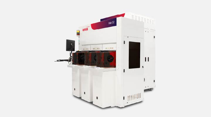
The Iris G2 system is an advanced optical metrology tool for both common and critical thin films for advanced node, mature and specialty devices, enabling manufacturers to increase transistor speed, reduce power consumption and improve reliability.

A suite of OCD modeling software and computing hardware that enables the full capability and connectivity across all Onto OCD and thin film metrology systems, including Atlas, Aspect, Iris and IMPULSE systems.
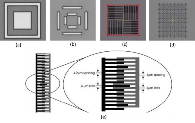
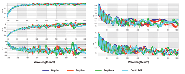
Hybrid bonding enables ultra-dense 3D memory interconnects with up to 1,000x more connections than microbumps. Achieving high yield requires stringent process control, including monitoring topography and detecting particles, cracks and voids. Measuring dishing in copper pads provides valuable insight into surface conditions. Together, these process control insights contribute to improved device reliability and performance.

As demand grows for high-performance computing (HPC) and AI-driven applications, manufacturers are turning to hybrid bonding to enable the ultra-dense 3D integration required for next-generation chip architectures. This advanced packaging technology presents significant process challenges. Surface preparation must be precisely controlled to eliminate particles, excess recess, and copper pad dishing, all of which can compromise bond quality. During pre-annealing, particle-induced gaps and wide bonding gaps can prevent proper wafer contact. Post-annealing, the formation of dielectric and metal voids introduces further risks to electrical performance and long-term reliability.
The Iris S system is a versatile platform solution for the advanced packaging and specialty market, supporting 150mm, 200mm and 300mm wafers. It provides thin and thick film, OCD and wafer bow and film stress measurements.
The IMPULSE V system helps to advance CMP processing with enhanced wavefront technology and AI-driven analytics, delivering over 2X precision improvement and faster solutions, crucial for next-gen semiconductor manufacturing demands.

The Dragonfly G3 system is resetting the industry’s expectations for throughput, accuracy and reliability. Combining 2D and 3D technologies, the system detects yield-robbing defects and measures features critical for today’s front-end and packaging technologies.

The Aspect System is a revolutionary in-line, non-destructive infrared optical critical dimension (IRCD) system measuring Z-dimension profiling of high aspect ratio structures to enable critical process control. It meets the needs of leading-edge customers with its high speed and process coverage.
As your partner for innovative solutions, we’re always here for you.
Discover how our cutting-edge semiconductor solutions are engineered to meet your most complex challenges: delivering performance, reliability and innovation where it matters most.
"*" indicates required fields