

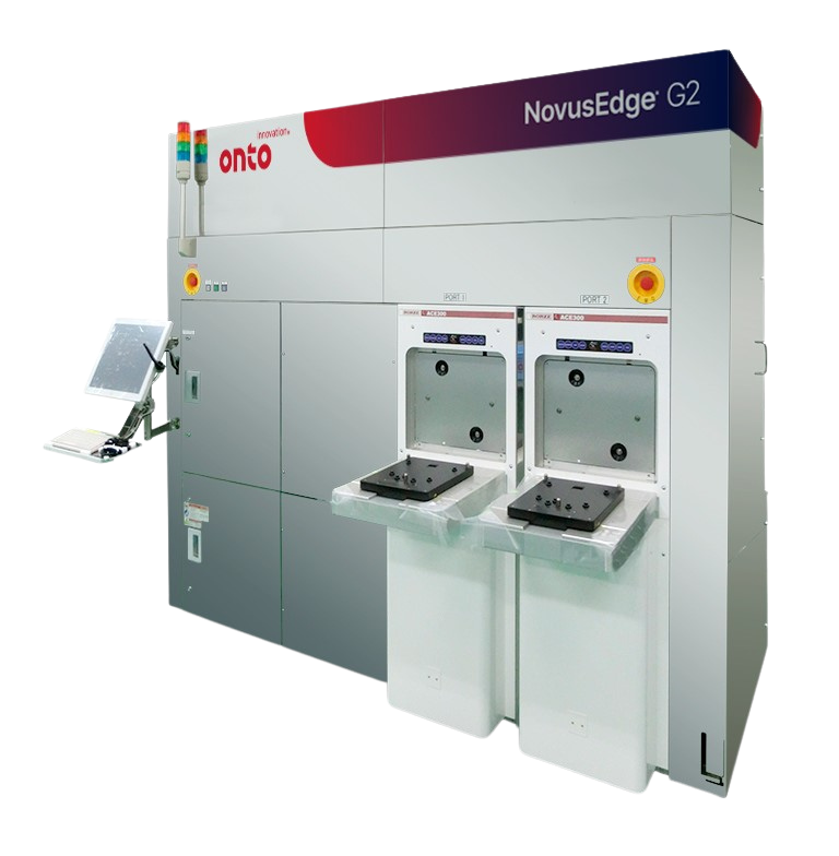
NovusEdge® G2 System
The NovusEdge G2 System offers fast, reliable edge, notch and backside inspection for 300mm unpatterned wafers, utilizing modular configurations.
Product Overview
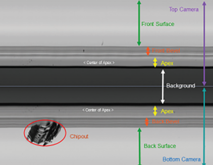
The NovusEdge G2 System provides high sensitivity inspection for the edge and backside of unpatterned wafers for current and advanced nodes. Configurable modules on the same automation platform increase throughput while maintaining a small footprint for improved cost of ownership. The edge-gripping handling solution for both automation platform and the inspection modules provide desired cleanliness required for manufacturing. Optional high-sensitivity notch inspection can be added. Defects are automatically classified and binned at run time to reduce manual review.
Designed as a multipurpose inspection and sorting system for end of line outgoing quality inspection of 300mm unpatterned wafers, the system identifies, inspects and sorts wafers according to recipes.
The NovusEdge G2 system offers higher sensitivity than the previous generation, with sub-micron resolution and increased throughput by over 15%. User interaction is simplified, and the new electrical design consumes less power.
Applications
- In-process unpatterned wafer sorting (grading)
- Incoming wafer inspection
- Tool qualification and monitoring
Featured Markets

Hunting For Macro Defects: The Importance Of Bare Wafer Inspection

Do you have a NovusEdge G2 system question? Let’s talk!
As your partner for innovative solutions, we’re always here for you.
Discover how our cutting-edge semiconductor solutions are engineered to meet your most complex challenges: delivering performance, reliability and innovation where it matters most.
Let’s Talk
"*" indicates required fields
Abstract
A vital component of modern communication systems, bulk acoustic wave resonators (BAW) function as filters, oscillators, and sensors. In a BAW device, the acoustic waves are confined within a specific region to achieve efficient resonance. The air ring structure, including the edge air layer structure, prevents acoustic energy from leaking. However, measuring the critical dimensions (CD) of edge air layers is challenging. In this paper, we will show how Onto Innovation’s IVS™ 220 optical overlay and CD metrology system can measure the edge air layer structure using a CD step application. The IVS 220 system provides good repeatability and high throughput [130 wph, five (5) fields, one (1) site per field]. In addition, the IVS 220 system also can be used for overlay measurement, CD measurement (including angle CD and diameter of the circle or hole), and Z height measurement.
You Have a Challenge? Let’s talk.
We’d love to connect with you.
Looking to learn more about our innovative solutions and capabilities? Our team of experts is ready to assist you. Reach out today and let’s starts a conversation about how we can help you achieve your goals.
Let’s Talk
"*" indicates required fields
When it comes to data accessibility, the terms “secure” and “share” seem like two diametrically opposed words. Conventional wisdom would suggest that any effort to secure data would involve limiting access to that data, while sharing data would involve opening up access to that data for others to view and use.
As it turns out, semiconductor operations need to do both.
On the one hand, semiconductor companies often need to share data so others can leverage data for problem solving and improve their overall manufacturing processes. On the other, these companies need to know their data is secure and free from data leaks resulting in lost IP or negating a competitive advantage. The solution: secured data sharing.
All great voyages must come to an end. Such is the case with our series on the challenges facing the manufacturing of advanced IC substrates (AICS), the glue holding the heterogeneous integration ship together.
In our first blog, we examined how cumulative overlay drift from individual redistribution layers could significantly increase overall trace length, resulting in higher interconnect resistance, parasitic effects and poor performance for high-speed and high-frequency applications. To address this, layer to layer overlay performance data needs to be monitored at each layer. If the total overlay error exceeds specifications at any process step, and at any location on the panel, corrective action must be taken to mitigate the drift in total overlay.
For this second installment, we explored the issue of AICS package yield and its importance in fostering a cost-effective, production-worthy process. Unlike most fan-out panel-level packaging (FOPLP) applications, AICS has relatively few packages per panel. This enormous disparity impacts yield calculations dramatically. In the AICS production process, the main challenge is the real-time tracking of yield for every panel, at every layer, throughout the fab. The solution: using advanced automatic defect classification (ADC) and yield analytics to quickly address errors.
In this final article of the series, we explore how overlay correction solutions compensate for panel distortion effects induced by copper clad laminate (CCL) processing, which impacts yield and final package performance.
In our previous blog, I talked about the essential factors that a company must consider in leveraging cloud resources to accelerate their goals. The objective here is not just about putting some of the workload in the cloud; rather, it is about realizing the transformation adopting cloud technologies will bring about. In particular, it is more important to think of the cloud not only as a set of infinitely scalable services and resources but as the underlying technologies and best practices that can be adopted as a framework for your software architecture in general. While I don’t mean to belabor the point, adopting the cloud in a manner where it can truly unlock operational efficiencies and leverage its advantages is truly an organizational change.
Business strategy
You’re unlikely to see the phrase “we want to use cloud more” in any organization’s strategic plans. However, the cloud can play a strategic role in expediting innovation; optimizing and reducing IT costs; helping a company meet the scalability demands required as new services, products or markets are launched; and making data accessible and actionable across disciplines in the organization. The cloud can assist with predictive maintenance, supply chain transparency, testing, quality, process automation and smart manufacturing. The chart from Accenture below captures the broad areas where the cloud can be leveraged easily in support of an organization’s goals (Fig 1).
It’s no secret the cloud is a driving force powering the digital transformation. However, cloud adoption is rarely a one-size-fits-all operation. Even when done correctly, it can bring about company-wide transformations unique to each organization. At the very core, the move to the cloud is akin to a culture change, and understanding these changes can make the transition successful. The following factors are worth considering:
Business strategy
Your cloud journey should start with company buy in, a budget and a roadmap with clear objectives, outcomes and performance metrics. The objectives need to be realizable and long-term. Having the right stakeholders involved helps keep initiatives going in the organization and ensures that the effort is not done in a siloed manner. Milestones, playbacks, celebrating successes and recognizing failures transparently is extremely important. Having the ability to change the organizational design to best leverage a transition is also necessary.
Choosing a platform
Plenty of providers can help you realize what best fits your organization. The key, however, is to know the strengths and weaknesses of each platform. While a relocation from one provider to another is possible, you generally are in partnership with a provider for the long haul. Remember, you are not just provisioning resources — it’s about data, data-lifecycle, applications, leveraging services, cost, building up expertise and other factors.