
As technology nodes shrink, end users are designing systems where each chip element is being targeted for a specific technology and manufacturing node. While designing chip functionality to address specific technology nodes optimizes a chip’s performance regarding that functionality, this performance comes at a cost: additional chips will need to be designed, developed, processed and assembled to make a complete system solution.
At back-end packaging houses in the past, a multi-chip module (MCM) placed various packaged chips on a printed circuit board. Today in the advanced packaging space, fabless companies are using an Ajinomoto build-up film (ABF) substrate as a method of combining various chips into a smaller form factor. As the push for increased density in smaller multi-chip module packages increases, process cost increases as well. Along with rising costs, the cycle times needed to process ABF substrates with ever more redistribution layers (RDL) also increases. Consequently, the need for back-end packaging houses to maintain process control and detect defects is going to be similar to what front-end fabs encountered in the 1990s.
Currently, substrates are 100µm to 150µm thick. As with front-end semiconductors, Moore’s law is going to come into play with advanced substrate packaging technology. Line width/interconnects are going to shrink, and the need to be able to control and detect feedback will grow.
Reticle exposure on a non-ridged substrate inherently will require better control for rotational, scaling, orthogonal and topology variation compensation. One solution is to use a feed-forward adaptive-shot technology to address process variations, die placement errors and dimensionally unstable materials. Such a solution uses a parallel die-placement measurement process, while advanced analytics provide a means to balance productivity against yield.
Displacement errors can be measured on a lithography tool, but the measurements are slow, typically taking as much time to conduct as the exposure. But moving the measurements to a separate automated inspection system and feeding those corrections to the lithography system can double throughput. In addition, yield software adds predictive yield analysis to the externally conducted measurement and correction procedures and increases the number of die included in the exposure field up to a user-specified yield threshold.
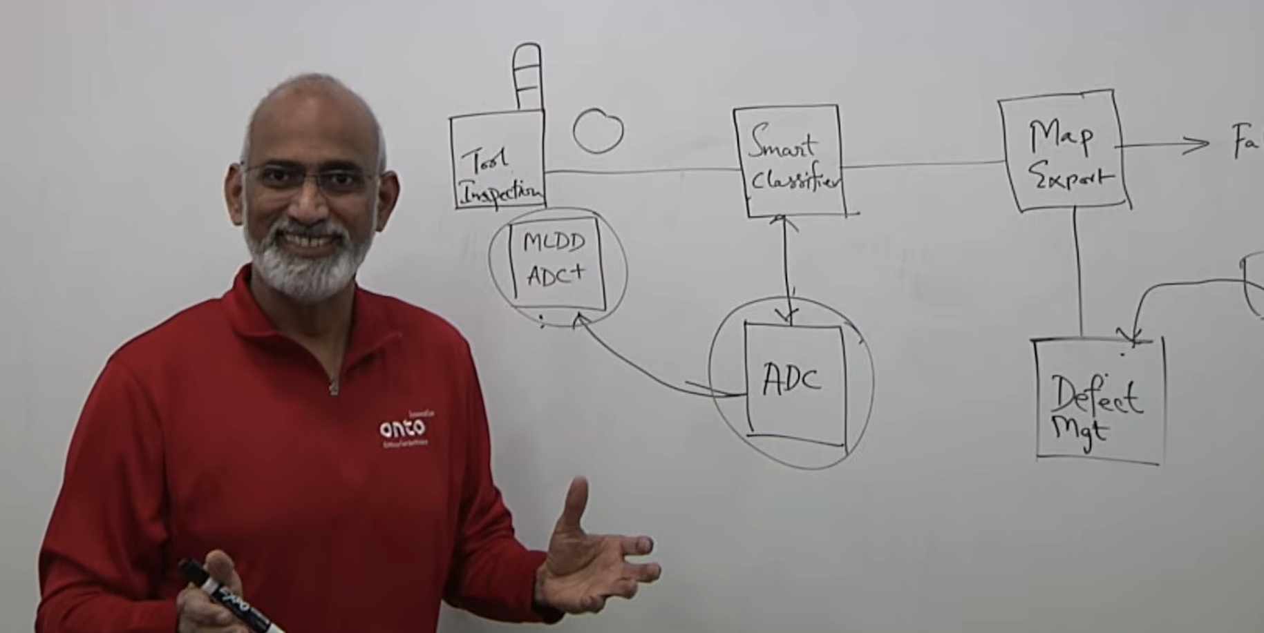
The following paper presents a case study describing how to improve yield and fab productivity by implementing a frequent pattern database that utilizes Artificial Intelligence based Spatial Pattern Recognition (SPR) and wafer process history. This is important because associating spatial yield issues with process and tools is often performed as a reactive analysis, resulting in increased wafer scrap or die loss that could be prevented. The implementation of fab fingerprint technology proactively generates a pareto of high impacting process steps and tools based on a pattern score, enabling the production team to concentrate more efficiently on yield limiting events.
Analysts are projecting strong growth in advanced packaging, with CAGR through 2026 approaching 7% across the segment; much higher for certain high-end technologies, including 3D stacking, embedded die, and fan-out. Outsourced assembly and test (OSAT) firms, which package finished die manufactured by independent device manufacturers (IDM) and foundries, will be challenged by the complexity of the advanced packaging processes and will face stiff competition, in many cases from their own customers. If they are to thrive, or perhaps just survive, they will need to embrace smarter manufacturing approaches.
The historical division between front-end device manufacturing and back-end packaging/testing is the result of their vastly different cost structures and process complexity. The relative simplicity of the back-end process led OSATs to compete primarily on price, seeking always to minimize costs and maximize volume. Simple processes were simple to control. The acquisition, storage, and analysis of process data were costs to be avoided wherever possible. Advanced packaging processes have introduced a host of new variables that must be controlled to ensure process yield and product reliability. Process data is no longer a cost to be avoided, but should be considered an essential asset to be leveraged to maximize profitability.
Meanwhile, as they accommodate increasingly complex processes, OSATs confront encroachment in their markets by sophisticated competitors who may also be their customers – IDMs and foundries who have outsourced a significant portion of their production to OSATs but have also maintained their own internal back-end capabilities. Advanced packaging processes have been described as the migration of front-end like processes to traditionally back-end applications. With this evolution, the advantage device manufacturers once had, by outsourcing assembly and test to avoid diluting their expertise with low-value processes, has greatly diminished. More importantly, these customers-turned-competitors are already comfortable with managing complex processes – they wrote the book. In addition to IDMs and foundries, substrate and printed circuit board (PCB) suppliers, electronic manufacturing services (EMS), original design manufacturers (ODM), and others see the opportunity presented by the significant growth forecasted for advanced packaging.
Data is the life blood of smarter manufacturing – acquiring it, storing it, organizing it, analyzing it, sharing it. Without leveraging it you are not just blind; in the competitive environment of semiconductor manufacturing, you will probably not survive. OSATs are not new to data collection and management. After all, testing is part of their name. But test data is product/function focused. In its simplest form it is go/no go. Functional testing may go beyond that, to measure how well it works, if for no other reason than to identify the best devices and sell them for premium prices. Smarter manufacturing requires data on a whole new scale – data that is both deep and broad.