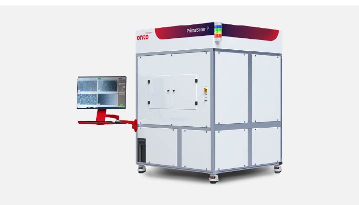
PrimaScan™ P System
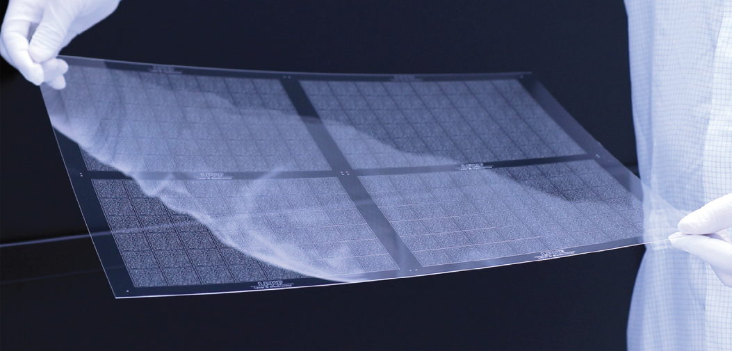
All-surface defect and contamination inspection for unpatterned glass panel substrates with imaging capability for panels up to 600x600mm in size.
The number of defects detected through inspection is exploding at each new process node. There are now millions of defects being identified on each wafer, but only a fraction of those can cause problems.

Sept 2 — Sept 4, 2026
Onto Innovation is a proud exhibitor at SEMICON Taiwan.
The PrimaScan wafer defect inspection system delivers a flexible, high sensitivity solution at the lowest cost of ownership per pass.
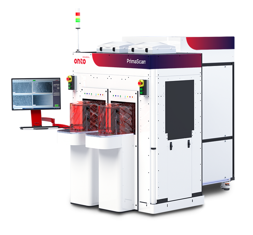
The PrimaScan system utilizes laser scatterometry and imaging techniques leveraging proprietary optics and sensing technologies for reliable inspection of nanometer sized defects on a variety of opaque and transparent/semi-transparent substrates suitable for either R&D or high-volume manufacturing environments. With multiple detection channels, the system can detect, measure, characterize and image surface particles, scratches, pits, bumps, surface contamination, film or bulk wafer stress, voids/inclusions, including chips and cracks at the wafer edge.
The PrimaScan system addresses challenges in both incoming wafer quality control and in inline process monitoring. Capable of handling multiple substrate materials, it uniquely addresses inline process defect and contamination monitoring in wafer-based production environments.
Designed with versatility in mind the PrimaScan system can handle a variety of wafer sizes and substrate types


As your partner for innovative solutions, we’re always here for you.
Discover how our cutting-edge semiconductor solutions are engineered to meet your most complex challenges: delivering performance, reliability and innovation where it matters most.
"*" indicates required fields
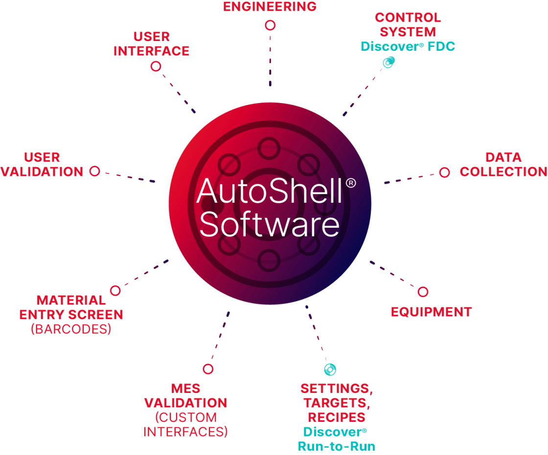
AutoShell software accelerates Industry 4.0 adoption by connecting multiple data sources throughout the fab in a single platform.
In a fast-changing industry, AutoShell software ensures competitiveness by seamlessly connecting systems, equipment and people in the factory. Its reliability and uptime make it essential for digital transformation.
AutoShell software unifies products, processes, equipment, stakeholders and facilities through versatile communication protocols across factory networks, optimizing limited IT resources. Its gateway, data acquisition tools, automation suite and multilingual development kit enable efficient data management and communication.
With over 10,000 systems across 500+ product types, AutoShell software empowers customers to execute factory operations without interruption, driving productivity and adaptability. It isn’t just software—it’s the backbone of the future-ready factory.


As your partner for innovative solutions, we’re always here for you.
Discover how our cutting-edge semiconductor solutions are engineered to meet your most complex challenges: delivering performance, reliability and innovation where it matters most.
"*" indicates required fields
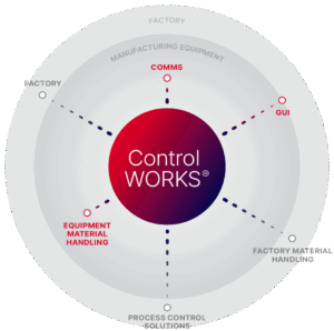
ControlWORKS software manages equipment-level material handling, factory communication, advanced scheduling and UI development through a comprehensive single machine control platform. This software increases product development efficiency and reduces time to market.
Next-generation technology nodes are advancing faster than process equipment development, challenging manufacturers to shorten product timelines. The ControlWORKS platform streamlines tool automation, allowing engineers to focus on innovation that drives market adoption. Its Object-Oriented Architecture supports swift development of diverse equipment types and processes. The Reusable Class Library enhances exception handling, communication and multitasking. Its SEMI® software compliant design adheres to industry standards (SECS/GEM, EDA, 300mm) and functions across multiple operating systems, including Windows, Linux and VxWorks. Together, these features empower efficient and scalable manufacturing, while ensuring compatibility with industry norms.
As your partner for innovative solutions, we’re always here for you.
Discover how our cutting-edge semiconductor solutions are engineered to meet your most complex challenges: delivering performance, reliability and innovation where it matters most.
"*" indicates required fields
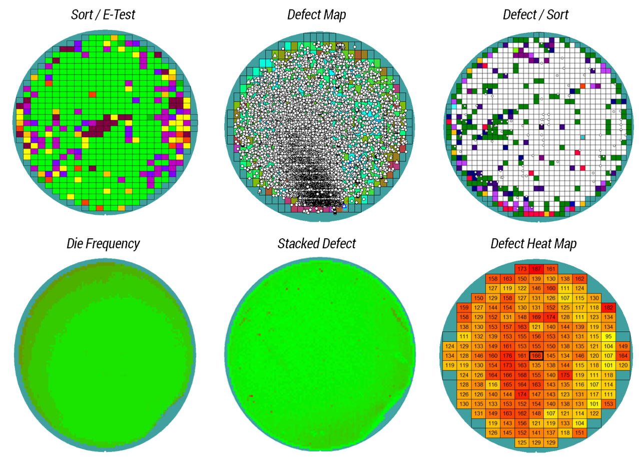
Discover Defect software provides actionable value to raw data through its intelligent, real-time analytics techniques. Inline monitoring, alarming and reporting is standard with all inspection tools, as well as offline fab-wide analysis with all licensed third-party tools.
Discover Defect software readily integrates into any wafer or panel production environment. It flexibly brings together all pertinent fab information, including defect, sort, metrology, wip, and electrical, into a single big data-capable solution. Its speed and up-time are world class.
Discover Defect software will pay for itself repeatedly by enabling its users to identify and solve problems, as well as to monitor and alarm on known areas of concern quickly and accurately. The product is designed to improve both throughput and yield while simultaneously reducing manufacturing costs.
Expand your yield analysis capabilities with the power of the Discover Yield software module. Discover Yield software’s patented data mining capabilities and advanced statistical analysis allow for highly sophisticated, interactive root cause analysis. Discover Yield software gives you the power to deep-dive into your data to uncover even the most difficult-to-identify systemic process issues.
Comprehensive mapping suite that covers all aspects of semiconductor processes
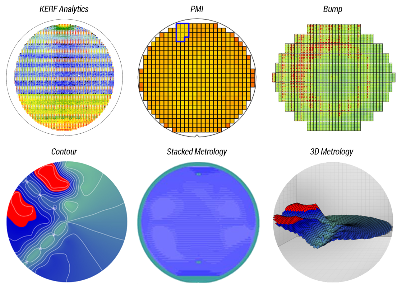
Targeted modules specific to customer challenges


As your partner for innovative solutions, we’re always here for you.
Discover how our cutting-edge semiconductor solutions are engineered to meet your most complex challenges: delivering performance, reliability and innovation where it matters most.
"*" indicates required fields
Discover Patterns software quickly and easily traces patterns back to yield-killing process issues.
Discover Patterns software combines sort and defect spatial patterns utilizing proprietary machine learning (ML) algorithms, to uncover hidden patterns that would have been otherwise lost. Segmentation allows users to eliminate noise and extract definitive patterns from a larger pattern or a seemingly random array of defects. Wafer stacking enables the handling of faint defect trends to more clearly isolate patterns.
Combining Discover Patterns software with the Discover Defect platform multiplies the value of your defect management infrastructure by intelligently identifying and acting upon known patterns in real time. It marks defects and die affected by patterns for deeper understanding of processes and reduces the need for human intervention.
Highlight all patterns, not just the dominant ones

As your partner for innovative solutions, we’re always here for you.
Discover how our cutting-edge semiconductor solutions are engineered to meet your most complex challenges: delivering performance, reliability and innovation where it matters most.
"*" indicates required fields
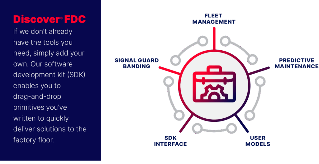
Discover FDC software is part of a robust data management suite, serving as the ideal gateway to digital transformation and unlocking Industry 4.0 best practices for impactful results.
Discover FDC software transforms tool sensor data into actionable insights. It empowers manufacturers to optimize fab efficiency, scaling seamlessly to high-volume manufacturing while reducing tool downtime by detecting anomalies early. With its diverse set of flexible controls and real-time data analysis, Discover FDC software enhances productivity, improves cycle time and increases equipment availability (OEE). Its user-friendly interface integrates advanced process control, allowing engineers to pinpoint issues and bring equipment online faster. Proven across processes and operational modules, it eliminates wasted time and energy by preventing idle tools and minimizing scrapped wafers. When connected to Discover Defect and Discover Yield software, Discover FDC software identifies meaningful correlations that drive even greater efficiency and production results. This robust solution redefines control, setting a new standard for achieving maximum enterprise-wide factory performance. That’s control, redefined.
As your partner for innovative solutions, we’re always here for you.
Discover how our cutting-edge semiconductor solutions are engineered to meet your most complex challenges: delivering performance, reliability and innovation where it matters most.
"*" indicates required fields