StepFAST® Software

An advanced feed-forward lithography software solution for fan-out panel level packaging that enhances yield and throughput by correcting die placement errors through external measurements, predictive analytics and adaptive shot control.

Product Overview

StepFAST® software is Onto Innovation’s advanced lithography software solution tailored for fan-out panel-level packaging, where die placement errors and material instability can significantly impact yield and productivity. StepFAST® software uses a feed-forward adaptive shot approach, integrating high-speed die placement measurements from the Firefly® system and applying real-time corrections to every shot of the JetStep® lithography tool. This external measurement strategy doubles throughput compared to traditional on-tool (self-metrology) methods. The software also incorporates predictive yield analysis, enabling dynamic adjustment of exposure field sizes to balance throughput and overlay accuracy. By automating reticle selection and optimizing field coverage, StepFAST® software ensures efficient panel exposure while minimizing registration errors—from ±50µm down to under ±3µm. With advanced analytics, StepFAST® software transforms lithography into a flexible, high-efficiency process, delivering substantial improvements in yield, throughput, and cost of ownership for panel-level packaging applications.

Applications

  • Panel-level packaging

Featured Markets

Related Products
View all
firefly_feat

Firefly® G3 System

Sub-micron automatic defect inspection with integrated 3D metrology for advanced IC substrates and panel level packaging.
View Product
jetstepx500_feat

JetStep® X500 System

Designed for advanced integrated circuit substrates (AICS) and other advanced packaging manufacturing applications, incorporating a 250mm x 250mm large field exposure area achieving 3μm L/S resolution with a large depth of focus.
View Product
jetsetps3500_feat

JetStep® S3500 System

Advanced packaging lithography system designed for fan-out panel level packaging, accommodating substrates up to 720mm x 600mm
View Product
Related Insights & Resources
View all
overlay

Addressing Copper Clad Laminate Processing Distortion Using Overlay Corrections

Learn more
Address-image

Addressing Total Overlay Drift In Advanced IC Substrate (AICS) Packaging

Learn more
fig-5_220126_110608

Outlier Control Technology and Feedforward Lithography Can Boost FOPLP Yield

Learn more
Picture1_210722_090506

Advanced Outlier Die Control Technology in Fan-Out Panel Level Packaging Using Feedforward Lithography

Learn more
overlay-results

Adaptive Shot Technology To Address Severe Lithography Challenges For Advanced FOPLP

Learn more

Do you have a StepFAST software question? Let’s talk!

As your partner for innovative solutions, we’re always here for you.

Discover how our cutting-edge semiconductor solutions are engineered to meet your most complex challenges: delivering performance, reliability and innovation where it matters most.

Let’s Talk

"*" indicates required fields

This field is for validation purposes and should be left unchanged.

IVS 380 System

The IVS 380 System delivers overlay, CD and z-height metrology for advanced packaging, power, compound semi and MEMS, offering world class performance and flexibility to accommodate substrates of different sizes and thickness without hardware changes.

IVS 380 System

Product Overview

The IVS 380 is an optical overlay, CD & z-height metrology system designed for high volume manufacturing, with SMIF (200mm substrate) or FOUP (300mm substrate) load ports compatibility. It handles various substrates for advanced packaging, including Si, glass and CCL, and accommodates sizes of 200mm and 300mm.

Building on the IVS family’s 40 years of experience in CMOS, MEMS and compound semiconductor applications, the IVS 380 system possesses the versatility to tackle overlay, CD and z-height measurements for diverse substrates and layers. It measures critical dimensions in the xy plane and the vertical z-heights of features like RDL metal lines, posts and bumps. The optics enable focus on mostly transparent materials such as photoresists and rough surfaces such as electroplated copper.

Applications

  • Critical Dimension
  • On Product Overlay
  • Specialty

3D Demo

Enter your information below and we’ll send you a unique passcode to view our IVS 3D Demo.

Related Products
View all
ivs280_feat

IVS 280 System

Overlay, CD and height metrology for 100mm-200mm wafers in the compound semiconductor, power devices, RF, MEMS and LED markets.
View Product

Do you have an IVS 380 system question? Let’s talk!

As your partner for innovative solutions, we’re always here for you.

Discover how our cutting-edge semiconductor solutions are engineered to meet your most complex challenges: delivering performance, reliability and innovation where it matters most.

Let’s Talk

"*" indicates required fields

This field is for validation purposes and should be left unchanged.

IVS 280 System

The IVS 280 system delivers overlay, CD and z-height metrology for 100mm-200mm wafers. It is designed to meet the challenging requirements of power, compound semi and MEMS segments.

IVS 280 System

Product Overview

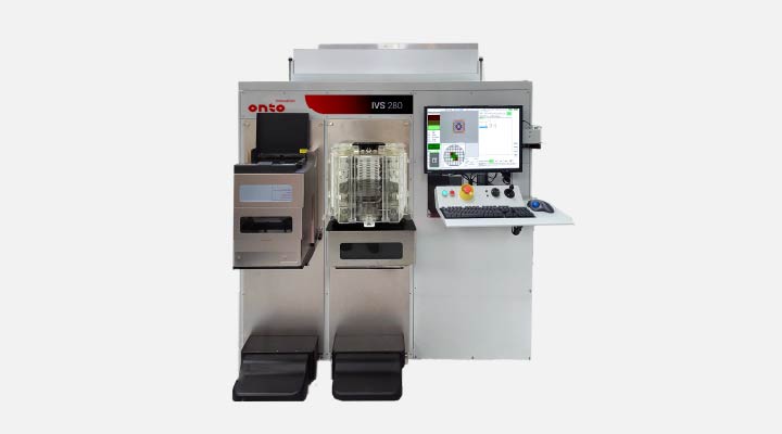
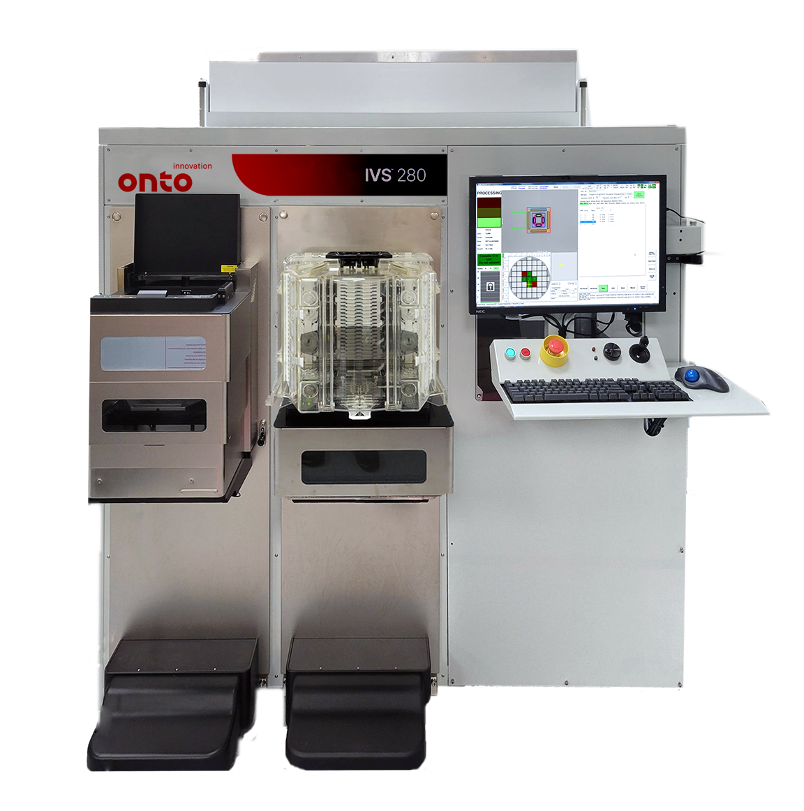
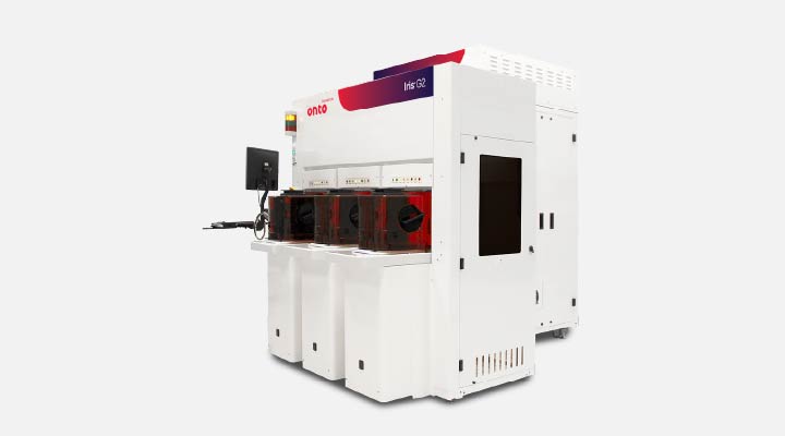
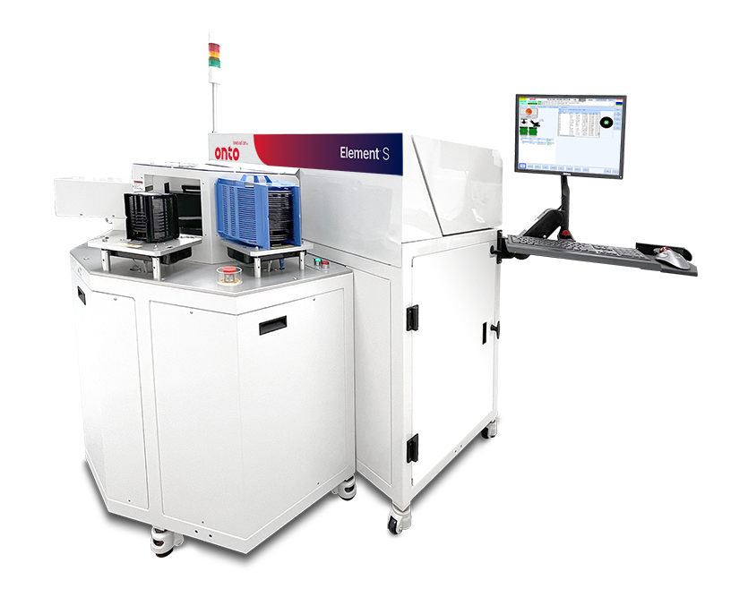
The IVS 280 system has been designed for ultimate precision, tool induced shift (TIS) and throughput for 100mm to 200mm wafers, with a mean time between failure (MTBF) > 2,000 hours. The IVS 280 system provides the same capability in a system designed for overhead track handling with full capability per SEMI® standards.

Flexibility is key in compound semiconductor processes, accommodating various wafer sizes, thicknesses, and compositions, including versatile wafer handling for Si, SiC, quartz, glass, GaAs, GaN, and LiNO3 wafers.

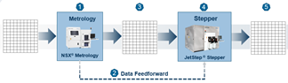
Its robust wafer handling and navigation system requires no operator assistance during recipe execution. The IVS 280 system enables wafer size changes without hardware alterations. Recipes and data remain stable over time. The system also supports recipe transfers from older IVS platforms like the IVS 200 and IVS 220.

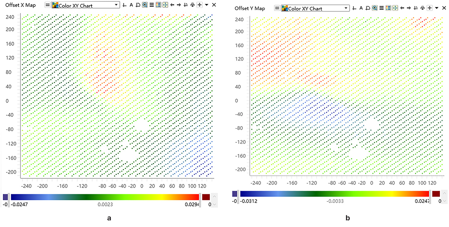
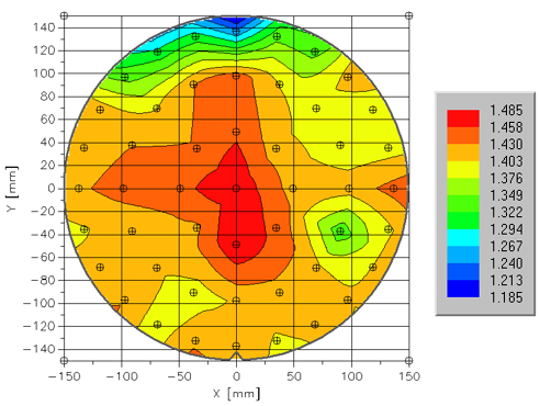
The demonstrated capabilities of the IVS system to perform with high precision and solid reliability set this system apart.

Applications

  • Critical Dimension
  • On Product Overlay
  • Z-Height

Featured Markets

3D Demo

Enter your information below and we’ll send you a unique passcode to view our IVS 3D Demo.

Related Products
View all
ivs280_feat

IVS 380 System

Overlay, CD and height metrology for 300mm wafers in the advanced packaging, compound semiconductor, power devices, RF, MEMS and LED markets.
View Product
Related Insights & Resources
View all
CD STEP APPLICATION IN EDGE AIR LAYER STRUCTURE MEASUREMENT FOR BULK ACOUSTIC RESONATOR

CD Step Application in Edge Air Layer Structure Measurement for Bulk Acoustic Resonator

Learn more

Do you have an IVS 280 question? Let’s talk!

As your partner for innovative solutions, we’re always here for you.

Discover how our cutting-edge semiconductor solutions are engineered to meet your most complex challenges: delivering performance, reliability and innovation where it matters most.

Let’s Talk

"*" indicates required fields

This field is for validation purposes and should be left unchanged.

Iris™ S System

The Iris S system is a versatile platform solution for the advanced packaging and specialty market, supporting 150mm, 200mm and 300mm wafers. It provides thin and thick film, OCD and wafer bow and film stress measurements.

Iris™ S System

Product Overview

The Iris S system delivers films metrology and advanced OCD capabilities for the specialty and advanced packaging segments. With a small footprint, it handles 150mm, 200mm, and 300mm wafer sizes, including thin, thick and bonded wafers. The system supports various materials such as Si, SiC, GaN and glass, addressing device-level challenges impacting performance and yield. Leveraging Onto’s Ai Diffract software, the Iris S system supports the most difficult on-wafer high value problems.

The Iris S system includes a dual-arm robot, high-precision stage, advanced pattern recognition, and high-speed focus for accurate positioning at high throughput. The dual channel optical architecture offers oblique incidence Mueller Matrix spectroscopic ellipsometry (MMSE) and normal incidence spectroscopic reflectometry (SR) in a broad wavelength range from UV to IR.

Based on Windows 10 OS and a 64-bit architecture, the Ai Diffract™ software interface and automation comply with SEMI standards. Onto’s model guided machine learning enables fast, flexible and robust film and OCD recipe setup.

Applications

  • Thin, thick and ultra thick film thickness
  • Trench/OCD metrology capabilities
  • Optical properties and composition solutions
  • Configurable for 6”, 8” and 12” wafer sizes
  • High warped wafer handling and stress measurements
  • Si, SiC, GaN and glass wafer handling
Related Products
View all
irisg2_feat

Iris™ G2 System

A high throughput common and critical thin film optical system for advanced and mature node devices.
View Product
impulse v_feat

IMPULSE® V System

Advanced high throughput integrated metrology system with AI-driven machine learning option. The system offers maximum sensitivity and accuracy to CMP process excursions and enables process engineers to establish APC control with high-accuracy feedback.
View Product
impulse+_feat

IMPULSE®+ System

Integrated metrology system offering maximum sensitivity and accuracy to CMP process excursions and enabling process engineers to establish APC control with high-accuracy feedback.
View Product
atlasv_feat

Atlas® V System

High performance OCD and thin film metrology for advanced GAA and memory devices.
View Product
atlasiii_feat

Atlas® III+ System

Versatile OCD and thin film metrology for mature and mainstream nodes.
View Product
Related Insights & Resources
View all
feb-2024-blog

Using OCD To Measure Trench Structures in SiC Power Devices

Learn more
adressing-trenches

Addressing Trench Structures and Larger Wafers for Power Devices

Learn more
Wei-Zhao-Star

A Star is Born: Gallium nitride and the coming age of compound semiconductors

Learn more

Do you have an Iris S system question? Let’s talk!

As your partner for innovative solutions, we’re always here for you.

Discover how our cutting-edge semiconductor solutions are engineered to meet your most complex challenges: delivering performance, reliability and innovation where it matters most.

Let’s Talk

"*" indicates required fields

This field is for validation purposes and should be left unchanged.

Element™ S System

The Element S system offers a unique combination of transmission and reflection-based technology, making it a valuable tool for dielectric monitoring.

Element™ S System

Product Overview

The Element S system is designed for the specialty market, specifically the smaller 100mm to 200mm wafer sizes used in the rapidly growing Si/SiC/GaN power device market. Building on the success of the Element Fourier transform infrared (FTIR) system, the Element S system can accurately measure thickness and free carrier concentrations in epitaxial layers up to five layers. This capability is essential for characterizing the thick epitaxial films required for next generation SiC power devices, which need thick epi layers for higher standoff voltage.

With its small spot size, the Element S system can conduct measurements up to the very edge of the wafer, maximizing die yield and enhancing productivity as power device customers transition to 200mm wafers. With improved sensitivity, an advanced multi-layer epi algorithm, and leading-edge multiple IR peak modeling, the Element S system provides critical and versatile capabilities for wafer and device makers in epi and film composition monitoring.

Applications

  • Multi layer Epi layer, transition zone thickness and substrate concentration
  • Power device EPI and buffer layer
  • BPSG, FSG, SiN, HSQ, SiON, SiCN, SiOC
  • Multiple IR peak metrics
  • Interstitial oxygen and substitutional carbon
  • Oxygen dose and Oxygen precipitate
Related Products
View all
elementg2_feat

Element™ G2 System

Transmission and reflection combined FTIR measurement for advanced epi thickness, film composition control and advanced IR modeling.
View Product
iris_feat

Iris™ S System

All-in-one solution for film metrology, OCD and stress measurements, tailored for advanced packaging and specialty segments.
View Product
MBIR System _feat2

MBIR System 

Advanced model-based infrared reflectometry (MBIR) metrology system for in-line monitoring of 3D structures used in V-NAND, CIS and power devices, as well as carbon hardmasks, dielectric compositions and epitaxial layer stacks.
View Product
Related Insights & Resources
View all
Using-FTIR-To-Improve-SiC-Power-Device-Performance

Using FTIR To Improve SiC Power Device Performance

Learn more
Wei-Zhao-Star

A Star is Born: Gallium nitride and the coming age of compound semiconductors

Learn more
ftir

Advanced Modeling In FTIR Offers New Applications For HVM

Learn more

Do you have an Element S system question? Let’s talk!

As your partner for innovative solutions, we’re always here for you.

Discover how our cutting-edge semiconductor solutions are engineered to meet your most complex challenges: delivering performance, reliability and innovation where it matters most.

Let’s Talk

"*" indicates required fields

This field is for validation purposes and should be left unchanged.

Element™ G2 System

The Element G2 system is a high-speed epitaxial layer metrology and wafer/film composition control system for wafer makers, advanced logic, DRAM and 3D NAND.

Element™ G2 System

Product Overview

The Element G2 system is designed for wafer suppliers to perform high speed impurity mapping and epi thickness measurements. It combines transmission and reflection-based technology and when paired with advanced IR modeling capability, it offers a unique approach to dielectric composition and film thickness monitoring. With improved sensitivity and cutting-edge algorithms, the Element G2 system is a critical metrology tool widely used for monitoring dielectrics such as BPSG, FSG, H in SiN, and more. Machine learning helps eliminate the need for monitor wafers in dielectric measurement.

The system features a crisp 2mm circular IR spot, a high sensitivity interferometer and advanced pattern recognition. Equipped with a Class 1, five-axis dual-arm edge grip wafer handling system, the Element G2 system delivers high precision and high throughput, even at the edge of the wafer.

Applications

  • Multi layer Epi layer, transition zone thickness and substrate concentration
  • Power device EPI and buffer layer
  • BPSG, FSG, SiN, HSQ, SiON, SiCN, SiOC
  • Multiple IR peak metrics
  • Interstitial oxygen and substitutional carbon
  • Oxygen dose and Oxygen precipitate
Related Products
View all
element s_feat

Element™ S System

Transmission and reflection combined FTIR Measurement for wafer, specialty devices, supporting 100-200mm wafer sizes.
View Product
iris_feat

Iris™ S System

All-in-one solution for film metrology, OCD and stress measurements, tailored for advanced packaging and specialty segments.
View Product
MBIR System _feat2

MBIR System 

Advanced model-based infrared reflectometry (MBIR) metrology system for in-line monitoring of 3D structures used in V-NAND, CIS and power devices, as well as carbon hardmasks, dielectric compositions and epitaxial layer stacks.
View Product
Related Insights & Resources
View all
FTIR_spie

Advanced FTIR Optical Modeling for Hydrogen Content Measurements in 3D NAND Cell Nitride and Amorphous Carbon Hard Mask

Learn more
ftir

Advanced Modeling In FTIR Offers New Applications For HVM

Learn more
Picture1

Expanded Material Metrology For Refined Etch Selectivities

Learn more

Do you have an Element G2 question? Let’s talk!

As your partner for innovative solutions, we’re always here for you.

Discover how our cutting-edge semiconductor solutions are engineered to meet your most complex challenges: delivering performance, reliability and innovation where it matters most.

Let’s Talk

"*" indicates required fields

This field is for validation purposes and should be left unchanged.