
For high-performance computing, artificial intelligence, and data centers, the path ahead is certain, but with it comes a change in substrate format and processing requirements. Instead of relying on the quest for the next technology node to bring about future device performance gains, manufacturers are charting a future based increasingly on heterogeneous integration.
But while heterogeneous integration promises more functionality, faster data transfer, and lower power consumption, these chiplet combinations, with different functionalities and nodes, will require increasingly larger packages, with sizes at 75mm x 75mm, 150mm x 150mm, or even larger.
To further complicate matters, these packages will also feature elevated numbers of redistribution layers, in some cases as high as 24 layers. And with each of those layers, the threat of a single killer defect, which would effectively ruin an entire package, increases. As such, the ability to maintain high yields becomes increasingly difficult.
The More than Moore era is upon us, as manufacturers increasingly turn to back-end advances to meet the next-generation device performance gains of today and tomorrow. In the advanced packaging space, heterogeneous integration is one tool helping accomplish these gains by combining multiple silicon nodes and designs inside one package.
But as with any technology, heterogeneous integration, and the fan-out panel-level packaging that often enables it, comes with its own set of unique challenges. For starters, package sizes are expected to grow significantly due to the number of components making up each integrated package. The problem: these significantly bigger packages require multiple exposure shots to complete the lithography steps for the package. Adding to this, multiple redistribution layers (RDL) may cause stress to both the surface and inside of the substrate, resulting in warpage. And then there is the matter of tightening resolution requirements and more stringent overlay needs.
When the subject of hybrid bonding is brought up in the industry, the focus is often on how this technique is used to manufacture CMOS image sensors (CIS), an essential device for today’s digital cameras, particularly those found in smartphones. As such, CIS is a common touchpoint given the ubiquity of mobile phones, whether you hold a product from Apple, Samsung or Huawei in your hands.
But while today’s CIS devices currently dominate the use of hybrid bonding, high-performance computing (HPC) is emerging as a new high-growth application for hybrid bonding. This is a result of the trend toward finer pitched interconnects in advanced 3D packaged memory technologies. In addition, the market share of high-end performance packaging, including both 2.5D and 3D packaging, is expected to be $7.87B by 2027, with a compound annual growth rate (CAGR) of 19% from 2021 to 2027, according to Yole Développement. As for 3D stacked packaging alone, it is expected to grow at a CAGR of 58% to 70% during the same period.
Using direct Cu-to-Cu connections instead of bumps and suitable for pitches less than 10μm, hybrid bonding often involves the direct stacking of two wafers, with the space between the two planarized surfaces approaching zero. Hybrid bonding has advantages over conventional micro-bumping, such as enabling smaller dimension I/O terminals and reducing pitch interconnects. But while both hybrid bonding and conventional micro-bumping support higher-density interconnect schemes, hybrid bonding is an expensive process compared to bumping and requires much tighter process control, especially in the areas of defect inspection, planarity measurement and void detection.
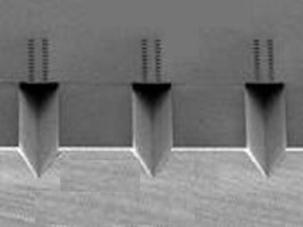
While wafer-to-wafer bonding has already been demonstrated for NAND devices and is currently used in CIS manufacturing for the integration of the imager layer and logic, DRAM manufacturers are also looking to adapt hybrid bonding to replace bumps. Utilizing a hybrid bonding interconnect scheme capable of reducing the overall package thickness by tens and possibly hundreds of microns in certain situations, HBM (high-bandwidth memory) die are vertically stacked in 4,8,12,16 die stacks. The gap between each die is about 30μm when bumps are used, but the gap is nearly zero with hybrid bonding.
Abstract
The growing demand for heterogeneous integration is driven by the 5G market. This includes smartphones, data centers, servers, high-performance computing (HPC), artificial intelligence (AI) and internet of things (IoT) applications. Next-generation packaging technologies require tighter overlay to accommodate larger package sizes with fine-pitch chip interconnects on large-format flexible panels. Heterogeneous integration enables device performance gains by combining multiple silicon nodes and designs inside one package. The package size is expected to grow significantly, increasing to 75mm x 75mm and 150mm x 150mm, within the next few years. For these requirements, an extremely large exposure field fine-resolution lithography solution was proposed to enable packages well over 250mm x 250mm without the need for image stitching, while exceeding the overlay and critical uniformity requirements for these packages.
One of the challenges of extremely large exposure field fine-resolution lithography is to achieve an aggressive overlay number. Formation changes experienced by the panel as a result of thermo, high-pressure and other fan-out processes shift the design location from nominal coordinates; this causes inaccurate overlay and low-overlay yield in the lithography process. Addressing this critical lithography challenge becomes an important task in heterogeneous integration.
In this paper, a 515mm x 510mm Ajinomoto build-up film (ABF)+copper clad laminate (CCL) substrate is selected as the test vehicle. We will analyze the pattern distortion of an ABF+CCL substrate to understand the distribution of translation, rotation, scale, magnification, trap, orthogonality and other errors in the substrate, and then use extremely large exposure field fine-resolution lithography to address the pattern distortion of the substrate. This demonstration will provide an analysis of panel distortion and detail how the extremely large exposure field fine-resolution lithography solution addresses panel distortion to achieve an aggressive overlay number.
The growing demand for heterogeneous integration is driven by the 5G market that includes smartphones, data centers, servers, HPC, AI and IoT applications. Next-generation packaging technologies require tighter overlay to accommodate a larger package size with finer pitch chip interconnects on large format flexible panels.
Fan-out panel level packaging (FOPLP) is one of the technologies that is able to achieve market requirements, but also faces several signification processes challenges. One critical challenge for FOPLP is die placement error, which is a result of the reconstitution process. Die placement error can cause high overlay error, which induces low overlay yield. To address this situation, site by site correction exposure with feedforward lithography is proposed. Site by site correction exposure can overcome the die placement error to achieve an acceptable overlay yield, and feedforward lithography is used to improve the throughput when using site by site correction exposure. An issue was observed when using feedforward site by site correction method: when one or more reconstituted dies suffered large displacement error, these large error dies affect the correctable accuracy of the site and induce poor overlay to all the dies in the site. To address this issue, which could induce poor overlay, advanced outlier control technology is proposed. Advanced outlier control technology is used for identifying the large error dies and processing these large error dies to prevent the situation.
In this paper, we demonstrated advanced outlier control technology with feedforward lithography on a selected test vehicle, which is a 510 mm x 515 mm panel. 400 simulation dies were built on this panel and part of the dies were designed with a large displacement error. The panel was processed using advanced outlier control technology with feedforward lithography in the demonstration. This demonstration showed how these two technologies integrated together and how this integration strategy worked for the FOPLP process. We also review and discuss the results for how this integration technology can maintain yield and throughput under such challenging conditions.
The growing demand for heterogeneous integration is driven by the 5G market that includes smartphones, data centers, servers, HPC, AI and IoT applications. Next-generation packaging technologies require tighter overlay to accommodate a larger package size with finer pitch chip interconnects on large format flexible panels.
Heterogeneous integration enables next-generation device performance gains by combining multiple silicon nodes and designs inside one package. The package size is expected to grow significantly, increasing to 75 x 75 mm and 150 x 150 mm, within the next few years. For these requirements, an extremely large exposure field with fine resolution lithography will enable packages well over 250 x 250 mm without the need for image stitching while exceeding aggressive overlay and critical uniformity requirements for these packages.
The lithography challenge to fulfill the need of heterogeneous integration is the limitation of exposure field size of the currently available solutions in the market. Multiple shots with stitching is used and this affects not only productivity performance but potential yield loss at the stitching boundary. Addressing the critical lithography challenges described above becomes an important task in heterogeneous integration, and an extremely large exposure field with fine resolution lithography is one of the best solutions for this task.
In this paper, a 515 mm x 510 mm panel is selected as the test vehicle, and we will demonstrate an extremely large exposure field with fine resolution technology on this panel. This demonstration provides the results and details about how this new technology will address the challenges of large package size processes.