
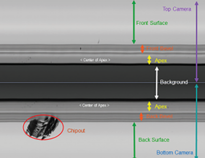
Discover® Defect Software
Integrated defect management system that works seamlessly with Onto tools and your entire enterprise, bringing data together for greater visibility and cleaner operation.

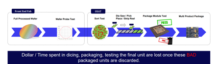
If you’ve been following the evolution of advanced packaging, you know that the industry is pushing boundaries like never before. From high-performance computing to industry-upending AI devices, the demand for smaller, faster, and more powerful chips is driving innovation at every level.

The 75th anniversary celebration of ECTC in Dallas showcases a remarkable evolution in advanced packaging technologies, revealing how semiconductor priorities have dramatically shifted. Rather than the relentless miniaturization of the smartphone era, today’s AI-driven applications demand larger packages with more functionality and sophisticated thermal management solutions.
Glass core substrates emerged as the star technology of the conference, with standing-room-only sessions demonstrating the industry’s intense interest in this promising material platform. The excitement is justified – glass offers superior dimensional stability and enables higher-density interconnects than traditional organic substrates. Meanwhile, co-packaged optics generated similar enthusiasm as engineers tackle the monumental challenge of powering AI server racks that consume between 0.5-1 megawatt each, making energy efficiency a critical concern.
The conversation with Onto Innovation’s Monita Pau begins at 1:10.
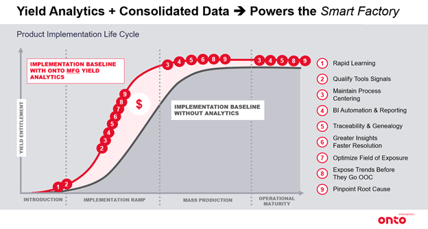
Yield Optimizer software is part of a comprehensive next-level data management portfolio. It reimagines manufacturing line control and analytics to explore the impact of previously invisible factors in day-to-day factory operation.
Yield Optimizer software is the next incarnation of analytics on the evolutionary scale. The software’s disruptive technology analyzes relationships between multivariant data and their complex interactions. By examining any set of conceivable inputs and outputs, Yield Optimizer software identifies the relationships and interactions that lead to positive operational changes. Easily understood visuals empower even casual users to understand what is important before making adjustments.
Yield Optimizer software evaluates multiple models and suggests the best one for the data. Using machine learning, it examines the interactions between in-process metrology readings and end-of-line test results for any semiconductor product family and recommends changes to the in-process metrology targets. When licensed as a service, it enables users to leverage an on-demand infrastructure to apply easily understood workflows for complex analytics without the overhead.
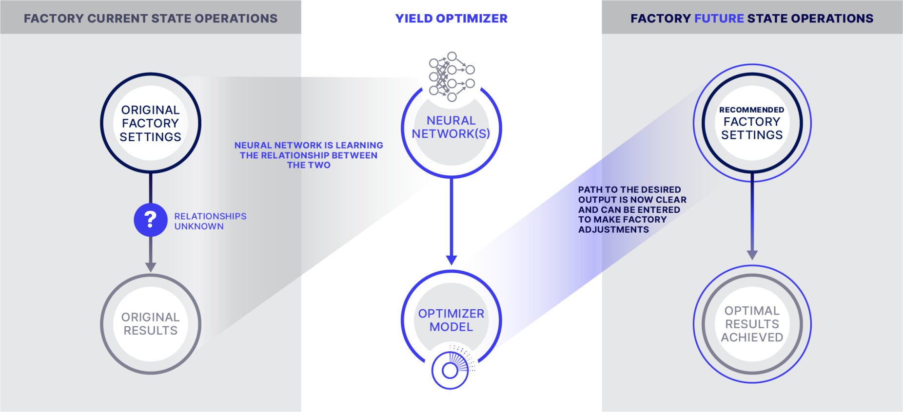
Neural networks model today’s data to achieve tomorrow’s in-line targets

Users across the fab benefit from Yield Optimizer software’s easy-to-apply analytics


As your partner for innovative solutions, we’re always here for you.
Discover how our cutting-edge semiconductor solutions are engineered to meet your most complex challenges: delivering performance, reliability and innovation where it matters most.
"*" indicates required fields
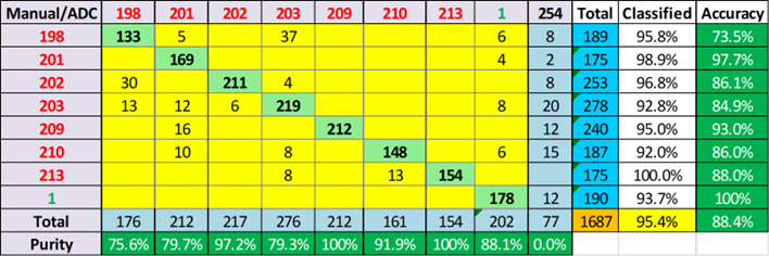
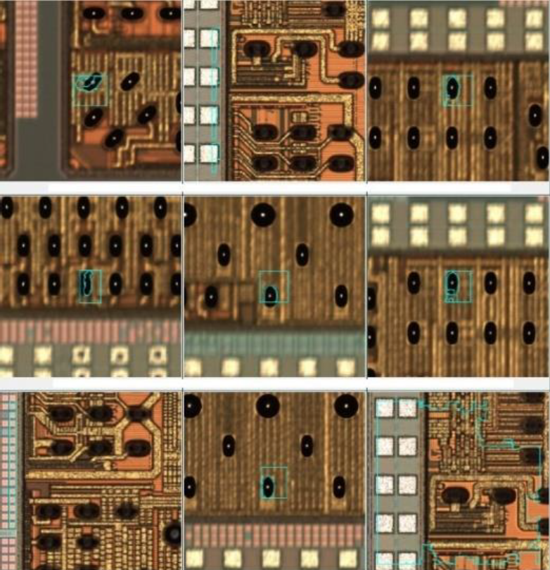
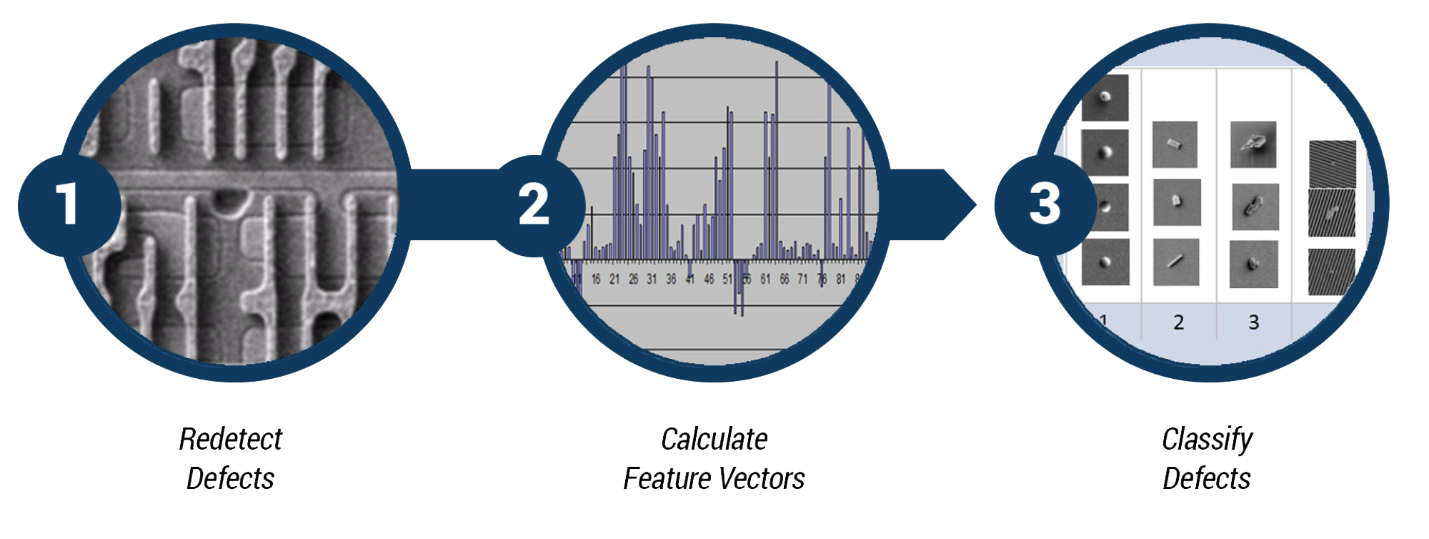
TrueADC software enhances defect classification accuracy and efficiency by combining deep learning, real-world defect modeling, and intuitive workflows—reducing manual review and improving decision-making across all wafers and surfaces.
TrueADC software sets a new standard in defect classification by combining advanced analytics with intuitive usability. Seamlessly integrated with Onto Innovation’s AOI tools and Discover platforms, TrueADC software enhances inspection value through a proprietary hybrid decision-making process across all wafers and surfaces.
With over 70% reduction in manual review, TrueADC software intelligently flags low-confidence defects as “unknown” to avoid misclassification. Its dynamic defect library method uses real defect examples—unlike traditional ADCs that rely on approximations—delivering more accurate and efficient results.
Supporting adder, repeater, SPR codes, and region-of-interest data, it enables precise tool sampling and binning. Operators can quickly classify new defects without altering recipes, while the software’s multi-engine mode leverages deep learning to reduce overkill and underkill.
From model development to identifying hard-to-isolate defects, TrueADC software empowers engineers with greater clarity, control, and confidence.


As your partner for innovative solutions, we’re always here for you.
Discover how our cutting-edge semiconductor solutions are engineered to meet your most complex challenges: delivering performance, reliability and innovation where it matters most.
"*" indicates required fields
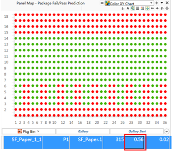
Discover Patterns software quickly and easily traces patterns back to yield-killing process issues.
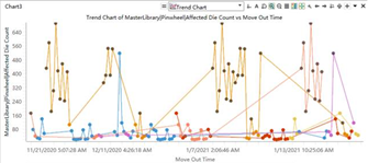
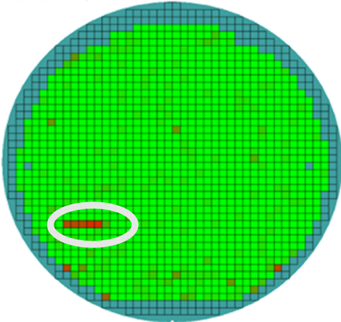
Discover Patterns software combines sort and defect spatial patterns utilizing proprietary machine learning (ML) algorithms, to uncover hidden patterns that would have been otherwise lost. Segmentation allows users to eliminate noise and extract definitive patterns from a larger pattern or a seemingly random array of defects. Wafer stacking enables the handling of faint defect trends to more clearly isolate patterns.
Combining Discover Patterns software with the Discover Defect platform multiplies the value of your defect management infrastructure by intelligently identifying and acting upon known patterns in real time. It marks defects and die affected by patterns for deeper understanding of processes and reduces the need for human intervention.
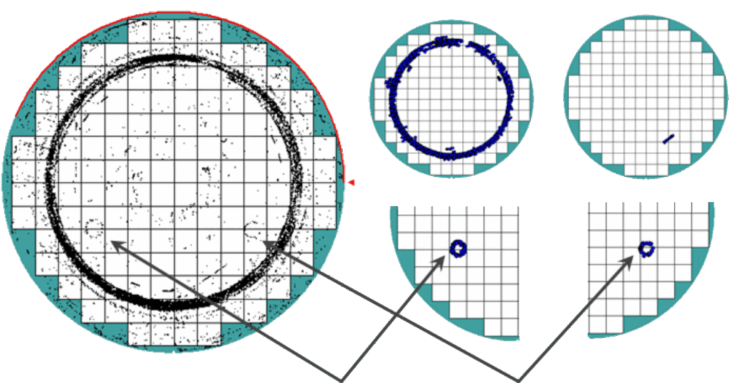
Highlight all patterns, not just the dominant ones
As your partner for innovative solutions, we’re always here for you.
Discover how our cutting-edge semiconductor solutions are engineered to meet your most complex challenges: delivering performance, reliability and innovation where it matters most.
"*" indicates required fields
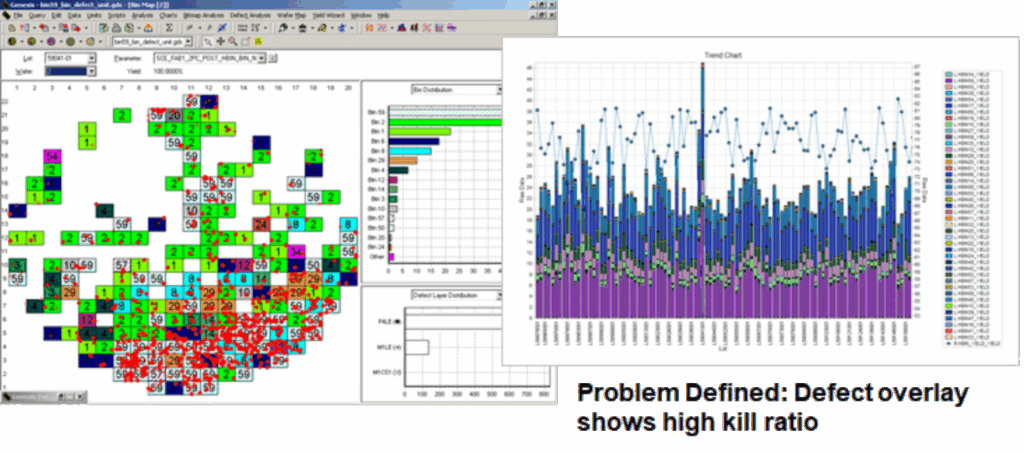
Discover Yield software is a complete yield management enterprise platform that combines parametric, defect and yield optimization with data mining and workflow development across all data sources from memory and design to assembly and packaging.
Discover Yield software helps reduce the time it takes to find root causes of yield excursions and enables manufacturers to broaden their analysis scope for better yield management.
The software includes data acquisition and integration, a development environment through workflow and scripting, and specialized analysis algorithms to identify domain-specific issues, such as data mining, spatial anomalies, wafer processing sequence problems, commonality of effects, system and random yield loss, chamber matching, tool events, traceability and more. In addition, Discover Yield software provides distinct tools – principal components and multivariate analysis of variance (MANOVA) – that allow systematic, simultaneous examination of multiple variables. Discover Yield software’s database architecture for genealogy uniquely supports value chain predictive analytics.
Improving baseline yield with analytics


As your partner for innovative solutions, we’re always here for you.
Discover how our cutting-edge semiconductor solutions are engineered to meet your most complex challenges: delivering performance, reliability and innovation where it matters most.
"*" indicates required fields
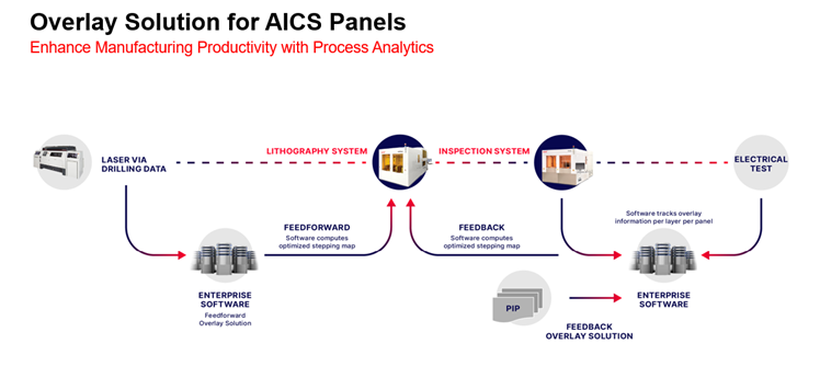
An advanced feed-forward lithography software solution for fan-out panel level packaging that enhances yield and throughput by correcting die placement errors through external measurements, predictive analytics and adaptive shot control.
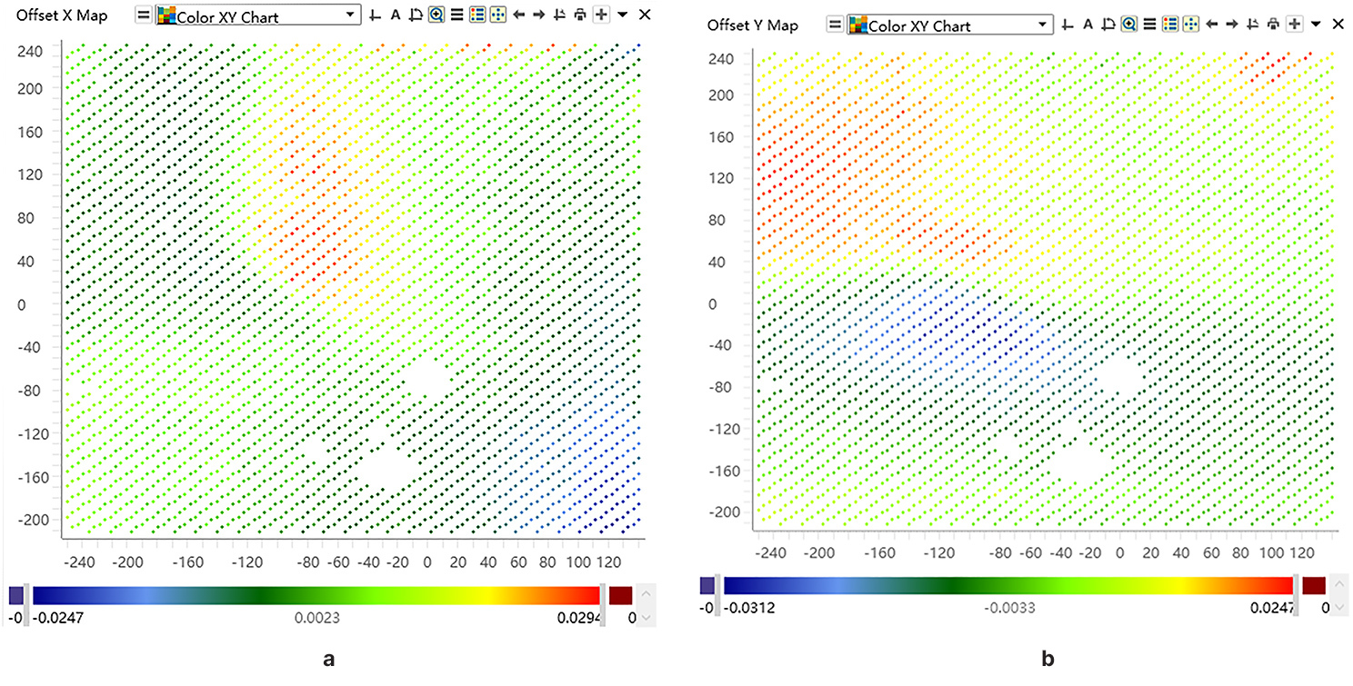
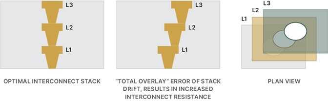
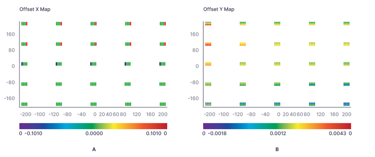
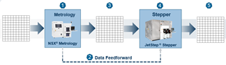
StepFAST® software is Onto Innovation’s advanced lithography software solution tailored for fan-out panel-level packaging, where die placement errors and material instability can significantly impact yield and productivity. StepFAST® software uses a feed-forward adaptive shot approach, integrating high-speed die placement measurements from the Firefly® system and applying real-time corrections to every shot of the JetStep® lithography tool. This external measurement strategy doubles throughput compared to traditional on-tool (self-metrology) methods. The software also incorporates predictive yield analysis, enabling dynamic adjustment of exposure field sizes to balance throughput and overlay accuracy. By automating reticle selection and optimizing field coverage, StepFAST® software ensures efficient panel exposure while minimizing registration errors—from ±50µm down to under ±3µm. With advanced analytics, StepFAST® software transforms lithography into a flexible, high-efficiency process, delivering substantial improvements in yield, throughput, and cost of ownership for panel-level packaging applications.
Die shift on reconstituted panels can significantly impact both productivity and yield. To address this challenge, we use a parallel die placement measurement process and advanced analytics to provide a means to balance productivity against yield. Our integrated lithography cell, featuring Firefly inspection, StepFAST software, and JetStep Lithography, delivers industry-leading throughput and yield for fan-out panel level packaging.
It is well understood that advanced packaging applications require high performance, low cost, increased functionality and improved reliability that 2.5D and 3D packaging solutions provide. Fan-out panel-level packaging (FOPLP) is one of the technologies that has the potential to meet these packaging requirements.
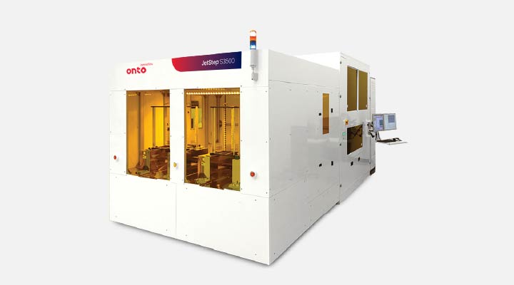
The JetStep S3500 system is designed to provide OSATS with a high-volume manufacturing advanced packaging lithography solution. For substrates up to 720mm x 600mm, it supports fan-out panel level packaging.
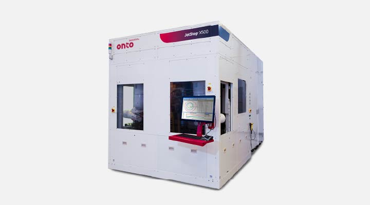
The JetStep X500 system is designed to provide AICS and OSAT manufacturers with a high-volume manufacturing lithography solution for heterogeneous integration. The JetStep X500 system exposes panel-type substrates made of CCL, FR4, composite, glass or other materials.
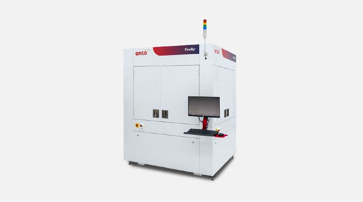
The Firefly G3 system provides automated inspection and 3D metrology for advanced IC substrates and panel level packaging, delivering high resolution and productivity for demanding applications like high-performance computing (HPC), artificial intelligence (AI), cloud computing and machine/deep learning.

An advanced feed-forward lithography software solution for fan-out panel level packaging that enhances yield and throughput by correcting die placement errors through external measurements, predictive analytics and adaptive shot control.
As your partner for innovative solutions, we’re always here for you.
Discover how our cutting-edge semiconductor solutions are engineered to meet your most complex challenges: delivering performance, reliability and innovation where it matters most.
"*" indicates required fields