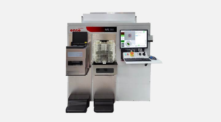
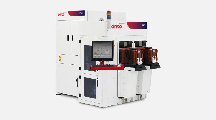
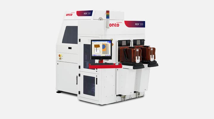
Sustainability

Sustainability in semiconductors drives progress in green energy and electric vehicles. Onto Innovation supports this shift with advanced metrology and process control for compound and power semiconductor manufacturing.

Jump to:

Green Energy

As the world shifts toward renewable energy sources, the demand for efficient power conversion and management is surging. This transition hinges on compound semiconductors like silicon carbide (SiC) and gallium nitride (GaN), which are essential for high-voltage, high-efficiency applications such as solar inverters and wind turbines. However, these materials present unique challenges in manufacturing, including defect detection and process variability.

Onto Innovation addresses these challenges through advanced metrology and inspection solutions tailored for the specialty semiconductor market. Our tools enable precise characterization of compound semiconductor wafers, ensuring quality and reliability in power devices. By enhancing yield and reducing waste, Onto Innovation plays a critical role in making green energy technologies more scalable and sustainable.

deco-bg-1 deco-bg-2

Electric Vehicles

Electric vehicles (EVs) are transforming transportation, but their performance and efficiency depend heavily on power semiconductors that manage energy flow between the battery and motor. These devices must operate reliably under high voltages and temperatures, making process control a critical factor in their production.

Onto Innovation supports this evolution with cutting-edge process control solutions that optimize the fabrication of power semiconductor devices. Our technologies help manufacturers detect defects early, monitor critical parameters, and maintain tight process windows—helping to ensure the high performance and safety standards EVs demand. By enabling more efficient and reliable power electronics, Onto Innovation is helping accelerate the global shift to electric mobility.

deco-bg-1 deco-bg-2
Related Products
View all
aspect_feat

Aspect® System

Advanced infrared optical critical dimension (IRCD) metrology system for high aspect ratio structures in 3D NAND, 2D & 3D DRAM, CIS and power devices.
View Product
atlasiii_feat

Atlas® III+ System

Versatile OCD and thin film metrology for mature and mainstream nodes.
View Product
celeroPL_feat

Celero™ PL System

Subsurface defect and crystalline defect inspection and classification in bulk and epitaxial III-V materials for application in power semiconductors.
View Product
discoverdefect_feat

Discover® Defect Software

Integrated defect management system that works seamlessly with Onto tools and your entire enterprise, bringing data together for greater visibility and cleaner operation.
View Product
discoveryield_feat

Discover® Yield Software

An advanced yield analysis toolkit that seamlessly integrates data from your entire enterprise, helping to prevent loss and better understand your process needs.
View Product
dragonfly g3_feat

Dragonfly® G3 System

Automated high speed sub-micron 2D inspection and 3D inspection/metrology for inline process control of pattern defects in next generation technologies for advanced packaging, specialty and OQA.
View Product
echo_feat

Echo™ System

Opto-acoustic film metrology for in-line, non-contact, non-destructive single and multi-layer metal film thickness measurements and material characterization on 150, 200, and 300mm substrates.
View Product
element s_feat

Element™ S System

Transmission and reflection combined FTIR Measurement for wafer, specialty devices, supporting 100-200mm wafer sizes.
View Product
f30_feat

F30™ System

Advanced macro inspection for front-end manufacturers.
View Product
iris_feat

Iris™ S System

All-in-one solution for film metrology, OCD and stress measurements, tailored for advanced packaging and specialty segments.
View Product
ivs280_feat

IVS 280 System

Overlay, CD and height metrology for 100mm-200mm wafers in the compound semiconductor, power devices, RF, MEMS and LED markets.
View Product
nsx330_feat

NSX® 330 System

2D automated defect inspection and sample 3D inspection for advanced packaging.
View Product
stepfast_feat

StepFAST® Software

An advanced feed-forward lithography software solution for fan-out panel level packaging that enhances yield and throughput by correcting die placement errors through external measurements, predictive analytics and adaptive shot control.
View Product
yieldoptimizer_feat

Yield Optimizer™ Software

Machine learning built with semiconductor manufacturing in mind.
View Product
Related Insights & Resources
View all
mask

Using Picosecond Ultrasonics To Measure Trench Structures In SiC Power Devices

Learn more
feb-2024-blog

Using OCD To Measure Trench Structures in SiC Power Devices

Learn more
Using-FTIR-To-Improve-SiC-Power-Device-Performance

Using FTIR To Improve SiC Power Device Performance

Learn more
adressing-trenches

Addressing Trench Structures and Larger Wafers for Power Devices

Learn more
optimizing

Optimizing Metal Film Measurement on IGBT And MOSFET Power Devices with Picosecond Ultrasonic Technology

Learn more
Default product image

Using Advanced Analytics To Meet ESG Goals

Learn more

Do you have a sustainability question? Let’s talk!

As your partner for innovative solutions, we’re always here for you.

Discover how our cutting-edge semiconductor solutions are engineered to meet your most complex challenges: delivering performance, reliability and innovation where it matters most.

Let’s Talk

"*" indicates required fields