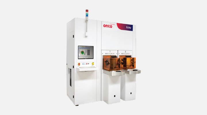
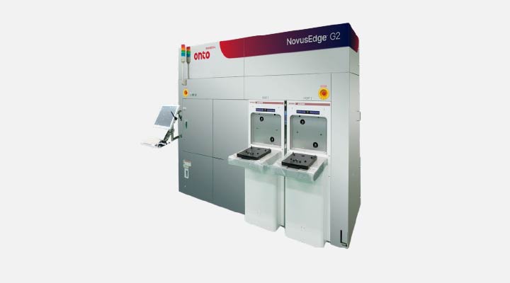
Connectivity

Connectivity is reshaping mobility and IoT. From 3D NAND to RF devices, Onto Innovation delivers advanced metrology and inspection solutions that enable high-performance, energy-efficient semiconductors for a seamlessly connected world.

Jump to:

Mobility

The future of mobility is defined by smarter, more connected, higher data throughput, vehicles and portable devices that demand high-performance, energy-efficient semiconductors. These applications rely heavily on advanced memory technologies like 3D NAND, which enable faster data access and greater storage density. However, manufacturing these complex structures introduces challenges in defect detection and layer uniformity.

Onto Innovation addresses these hurdles with advanced inspection and metrology solutions tailored for 3D NAND and compound semiconductor wafers. Our tools help ensure precise process control, enabling manufacturers to meet the rigorous demands of mobile applications. In the specialty device market, our solutions also support power management components like MOSFETs and MEMS, which are critical for battery efficiency and system reliability in mobile environments.

deco-bg-1 deco-bg-2

Internet of Things (IoT)

IoT is transforming industries by embedding intelligence into everyday objects—from smart homes to industrial automation. This explosion of connected devices requires ultra-low-power semiconductors, robust DRAM for real-time data processing, and reliable power management solutions.

Onto Innovation plays a pivotal role in enabling IoT by providing metrology and inspection solutions for DRAM and compound semiconductors used in power devices. Our tools support the production of high-yield, high-reliability components such as MOSFETs and MEMS, which are essential for IoT device efficiency and longevity. As the IoT ecosystem expands, Onto’s solutions help manufacturers scale production while maintaining the precision and reliability these applications demand.

deco-bg-1 deco-bg-2

5G/6G Communications

Wireless networks like 5G and emerging 6G technologies are revolutionizing how data is transmitted, demanding ultra-fast, low-latency communication. These systems rely on advanced RF components often based on unique materials or processes combined with compound semiconductors that must meet stringent performance and reliability standards.

Onto Innovation supports this evolution with cutting-edge metrology solutions that ensure the integrity of RF devices and materials. Our tools are critical for monitoring process variation and ensuring long-term reliability in high-frequency applications. By enabling precise control over complex semiconductor structures, Onto helps manufacturers deliver the performance and durability required for the connected world of today.

deco-bg-1 deco-bg-2
Related Products
View all
aspect_feat

Aspect® System

Advanced infrared optical critical dimension (IRCD) metrology system for high aspect ratio structures in 3D NAND, 2D & 3D DRAM, CIS and power devices.
View Product
atlasiii_feat

Atlas® III+ System

Versatile OCD and thin film metrology for mature and mainstream nodes.
View Product
atlasv_feat

Atlas® V System

High performance OCD and thin film metrology for advanced GAA and memory devices.
View Product
discoverai_feat

Discover® AI Software

A cutting-edge AI engine built for semiconductor manufacturing, providing actionable predictions and insights across nearly any process area.
View Product
discoverdefect_feat

Discover® Defect Software

Integrated defect management system that works seamlessly with Onto tools and your entire enterprise, bringing data together for greater visibility and cleaner operation.
View Product
discoveryield_feat

Discover® Yield Software

An advanced yield analysis toolkit that seamlessly integrates data from your entire enterprise, helping to prevent loss and better understand your process needs.
View Product
dragonfly g3_feat

Dragonfly® G3 System

Automated high speed sub-micron 2D inspection and 3D inspection/metrology for inline process control of pattern defects in next generation technologies for advanced packaging, specialty and OQA.
View Product
echo_feat

Echo™ System

Opto-acoustic film metrology for in-line, non-contact, non-destructive single and multi-layer metal film thickness measurements and material characterization on 150, 200, and 300mm substrates.
View Product
elementg2_feat

Element™ G2 System

Transmission and reflection combined FTIR measurement for advanced epi thickness, film composition control and advanced IR modeling.
View Product
element s_feat

Element™ S System

Transmission and reflection combined FTIR Measurement for wafer, specialty devices, supporting 100-200mm wafer sizes.
View Product
impulse v_feat

IMPULSE® V System

Advanced high throughput integrated metrology system with AI-driven machine learning option. The system offers maximum sensitivity and accuracy to CMP process excursions and enables process engineers to establish APC control with high-accuracy feedback.
View Product
impulse+_feat

IMPULSE®+ System

Integrated metrology system offering maximum sensitivity and accuracy to CMP process excursions and enabling process engineers to establish APC control with high-accuracy feedback.
View Product
irisg2_feat

Iris™ G2 System

A high throughput common and critical thin film optical system for advanced and mature node devices.
View Product
iris_feat

Iris™ S System

All-in-one solution for film metrology, OCD and stress measurements, tailored for advanced packaging and specialty segments.
View Product
ivs280_feat

IVS 280 System

Overlay, CD and height metrology for 100mm-200mm wafers in the compound semiconductor, power devices, RF, MEMS and LED markets.
View Product
ivs280_feat

IVS 380 System

Overlay, CD and height metrology for 300mm wafers in the advanced packaging, compound semiconductor, power devices, RF, MEMS and LED markets.
View Product
novudedge_feat

NovusEdge® G2 System

Unpatterned edge, notch and backside inspection.
View Product
nsx330_feat

NSX® 330 System

2D automated defect inspection and sample 3D inspection for advanced packaging.
View Product
ocdsolutions_aidiffract_feat

OCD Solutions

A suite of OCD modeling software and computing hardware offering comprehensive capabilities for inline metrology, offline recipe creation and fleet management.
View Product
precisionworx_feat

PrecisionWoRx® VX4 System

Wafer probe card test and analysis system.
View Product
primascan_feat

PrimaScan™ System

All-surface defect and contamination inspection for unpatterned wafer and blanket films, with imaging capability for opaque, transparent and semi-transparent wafers, reticles and piece parts.
View Product
Related Insights & Resources
View all
CD STEP APPLICATION IN EDGE AIR LAYER STRUCTURE MEASUREMENT FOR BULK ACOUSTIC RESONATOR

CD Step Application in Edge Air Layer Structure Measurement for Bulk Acoustic Resonator

Learn more
Importance-of-Secure-Data-may-2024

The Importance of Secure Data Sharing

Learn more
overlay

Addressing Copper Clad Laminate Processing Distortion Using Overlay Corrections

Learn more
Sky-High-Image

Sky High: More Thoughts To Consider Before Transitioning To The Cloud

Learn more
Default product image

Up and Away!: Clear-eyed considerations for your cloud-adoption journey

Learn more
Default product image

Paving the Way for 5G: RF Filter Process Monitoring and Control Using Picosecond Ultrasonic Metrology

Learn more
CSTIC-RF

Advantages of Picosecond Ultrasonic Technology for Advanced RF Metrology

Learn more
Lightbulb-with-connecting-dots-scaled

The Big Squeeze – Why OSATs Need to Work Smarter

Learn more
Metrology-for-RF

Full Metrology Solutions for Advanced RF with Picosecond Ultrasonic Metrology

Learn more

Do you have a connectivity question? Let’s talk!

As your partner for innovative solutions, we’re always here for you.

Discover how our cutting-edge semiconductor solutions are engineered to meet your most complex challenges: delivering performance, reliability and innovation where it matters most.

Let’s Talk

"*" indicates required fields