

Specialty
The specialty market spans multiple device applications and wafer sizes, necessitating a specialized understanding of how key process steps or films impact device performance and yield.
The high-volume production of specialty devices spans wafer sizes from 150mm to 300mm and includes CMOS Image Sensors (CIS), power management and switches, Micro-electro-Mechanical Systems (MEMS), analog and photonics device application segments. The device level applications covered in these segments rely on unique processes such as deep trench etch, thick or piezo films processing or a combination of specialized process steps to deliver key device functionality. Whether dealing with critical dimensions and profiles of high aspect ratio trenches, or thick film technologies, the challenges faced for process control are broad. To address this, Onto Innovation has enabled its lineup of process control products with dedicated process requirements in mind, while delivering low cost of ownership and improving overall device performance and yield.
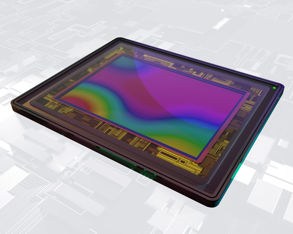
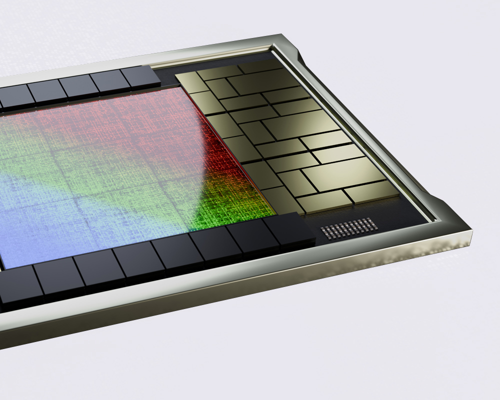
CMOS Image Sensor (CIS)
CIS devices are in our phones, cars and many applications even unknown to us. They are complex devices to manufacture and require specialized process steps to ensure high performance and yield. CMOS sensors must balance sensitivity, noise reduction and dynamic range to produce clear and accurate images, which require sophisticated design and manufacturing techniques. As devices become smaller, integrating high-performance CMOS sensors into compact spaces without compromising functionality is increasingly complex. This miniaturization also demands advanced fabrication processes to ensure the sensors are both efficient and reliable. CMOS image sensors must be cost-effective to produce. The manufacturing process involves precise, and often expensive, lithography and doping techniques. Ensuring high yield while minimizing defects is crucial to keeping production costs down. To stay competitive in this rapid pace of technological advancement, CMOS sensor manufacturers must continuously innovate. This requires significant investment in research and development to push the boundaries of what these sensors can achieve. Onto Innovation’s commitment to the application of advanced process control technologies means customers can continue to push the boundaries of device performance without sacrificing yield or cost per wafer.


Power Device Technologies
Developing power devices, high power switches, power management ICs, and more presents several complex challenges. One of the foremost critical challenges is achieving high efficiency. Power devices must convert electrical energy with minimal losses which requires optimizing their design and materials. Innovations in semiconductor materials, such as silicon carbide (SiC) and gallium nitride (GaN), are crucial for enhancing efficiency and performance.
Manufacturing precision is also a significant hurdle. Power devices require exacting fabrication processes to ensure they meet stringent performance standards. This involves sophisticated techniques like epitaxial growth and ion implantation which must be meticulously controlled to produce high-quality devices. The rapid pace of technological advancement demands continuous innovation. Manufacturers must invest in research and development to stay ahead in the competitive market, pushing the boundaries of power device capabilities.

Micro-Electro-Mechanical systems (MEMS)
MEMS devices integrate mechanical and electrical components, requiring advanced manufacturing techniques. To produce functional devices, it is crucial to ensure accuracy and consistency. MEMS devices must be made from materials that can withstand mechanical stress, thermal variations and chemical exposure. Finding materials that meet these criteria while being compatible with microfabrication processes is essential. The combination of these factors means that reliable process control technologies are essential to the fabrication of MEMS based devices in high volume manufacturing (HVM).
Integration of MEMS with electronic systems poses additional hurdles. These devices must interface seamlessly with electronic circuits, requiring sophisticated packaging and interconnection techniques. This integration ensures reliability and performance without compromising the device’s compact size. Cost-effectiveness is also a significant concern. The complex fabrication processes and high precision required for MEMS can lead to increased production costs. Manufacturers must find ways to optimize processes and materials to keep costs manageable. High aspect ratio etch processes, thick dielectrics, and piezo films, wafer bonding integration of mechanical layers and CMOS wafers, including a variety of wafer handling techniques have come to characterize modern MEMS production.

Analog Devices
Creating analog devices, such as amplifiers and sensors, involves several complex challenges. One of the primary difficulties is achieving high precision and accuracy. Analog devices must process continuous signals with minimal distortion and noise, requiring meticulous design and high-quality components. Ensuring signal integrity is crucial for the device’s performance.
Manufacturing consistency is also a significant hurdle. Analog devices require precise fabrication processes to ensure each unit meets stringent performance standards. Variations in manufacturing can lead to inconsistencies in device behavior, impacting overall reliability. High precision and quality requirements can lead to increased production costs. Manufacturers must find ways to optimize processes and materials to keep costs manageable while maintaining performance standards.
Onto Innovation’s range of process control technologies offers manufacturers of analog devices alternatives for low cost of ownership tools that deliver high precision capabilities to help ensure their HVM analog devices are made with reliable repeatability in precision and consistent performance.
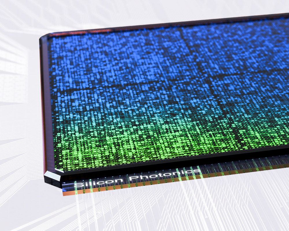
Silicon Photonics
Developing silicon photonics chips involves several significant challenges. One of the primary difficulties is integrating optical components with silicon-based electronic circuits. Silicon, while excellent for electronics, has limitations in optical applications, requiring innovative design and fabrication techniques to achieve efficient light transmission and modulation. Precision in manufacturing is also crucial. Silicon photonics chips require exacting fabrication processes to ensure the alignment and quality of optical components. Variations in manufacturing can lead to inconsistencies in performance, impacting the overall functionality of the chip. Achieving high data transmission rates while minimizing signal loss and noise is a significant hurdle. Silicon photonics chips must balance speed and accuracy, requiring advanced materials and design strategies to optimize performance. The complex fabrication processes and high precision required for silicon photonics can lead to increased production costs. Manufacturers must find ways to optimize processes and materials to keep costs manageable. Onto Innovation’s portfolio of metrology and inspection tools enables manufacturers of silicon photonics devices the ability to accurately manufacture active and passive waveguide components in a variety of materials while also confirming the alignment accuracy of coupled fiber components.

Do you have a specialty question? Let’s talk!
As your partner for innovative solutions, we’re always here for you.
Discover how our cutting-edge semiconductor solutions are engineered to meet your most complex challenges: delivering performance, reliability and innovation where it matters most.
Let’s Talk
"*" indicates required fields