

From consumer products to industrial applications, augmented reality (AR)/mixed reality (MR) technology is one of the most innovative interactive technologies on the market today. By overlaying digital information onto the physical world, AR/MR technology improves how people see, understand, and interact with their environment in real time. The industrial applications alone are cause for celebration, whether this technology is being used for training, assembly, or troubleshooting.
Be that as it may, one of the most significant challenges facing AR/MR lies in manufacturing the photonic components that control how light is generated, diffracted, guided, and delivered to the human eye.
An AR display usually consists of a light engine and an optical combiner. The light engine serves as a display image source, while the combiner delivers the displayed images to the viewer’s eye and transmits environment light (Figure 1). Surface relief grating (SRG) waveguides play a role in these optical combiners by coupling display light into, expanding it within, and diffracting it out of a transparent substrate toward the eye of the intended viewer. This component must deliver precise diffraction behavior while remaining transparent, lightweight, and scalable for high-volume manufacturing (HVM).
Balancing optical performance and manufacturability, however, places significant demands on fabrication and process control. Faced with this obstacle, device makers require solutions capable of addressing any negative impacts to launch timelines, unit costs, and OEM qualification.

Figure 1. Diagram of SRG waveguide-based AR display.
In this article we will discuss ways SRG manufacturers can address these challenges with an integrated process control solution tailored for the HVM of SRG. The solution combines optical critical dimension (OCD) metrology for the critical parameters of SRG such as grating depth, slanted angle, and periods; picosecond ultrasonic technology for the metal film thickness measurement; image‑based overlay (IBO) for precise overlay control in HVM specialty devices; and an automated optical inspection for defects integrated throughout the entire manufacturing process.
With these tools combined in a closed‑loop process control strategy, manufacturers have a framework that enables the consistent manufacturing of full‑color SRG waveguides capable of meeting the stringent optical and mechanical requirements of next‑generation AR/MR devices.
Navigating the Ramp to HVM
By coupling light into and out of a transparent substrate through precisely engineered diffraction gratings, SRG waveguides can deliver wide field‑of‑view, high brightness, and compact form factors. Unfortunately, manufacturers of SRG waveguides must face a host of challenges arising from multi‑layer and often double‑sided fabrication, with sub‑100nm alignment tolerances across large‑area substrates, if they hope to transition to HVM. The impact of these challenges, however, only grows as the manufacturing process goes on, increasing yield variability and making it difficult for makers of SRG components to meet the requirements expected by tier-one AR/MR customers.
To begin with, let’s turn to grating geometry. Manufacturers must control for period, depth, and slanted angle to ensure diffraction efficiency and uniformity across the field. Additionally, makers of these components must maintain proper thickness uniformity to avoid phase errors and color shifts; as such, thin‑film processes like mask deposition and etching must maintain exceptional thickness uniformity. Third, manufacturers must also maintain overlay accuracy between lithography steps, and they must do so within a fraction of the design tolerance to preserve red, green, and blue (RGB) multi‑period grating registration and double‑sided alignment. Finally, defect control is essential in the manufacturing process. After all, particles, scratches, and etch anomalies can cause scattering, reduce optical efficiency, and degrade image quality. Not surprisingly, the manufacturing process features a number of consequential steps (Figure 2).
In many cases, the process begins with the deposition of a chromium (Cr) hard mask on a SiO₂ substrate, followed by spin coating a resist layer. For master fabrication, electron beam lithography or deep ultraviolet lithography is used to pattern the grating structure. The resist pattern is then transferred to the Cr layer using a dry etching process, after which the residual resist is removed, leaving the Cr layer to serve as an etching mask for reactive-ion beam etching (RIBE). During RIBE, ionized argon beams are directed toward the substrate at an oblique angle to form the slanted grating profile. Once the target etch depth is achieved, the Cr layer is removed by chemical wet etching.
For HVM, the fabricated master grating is replicated using nanoimprint lithography (NIL) production due to its low cost and high throughput. In this process, the master pattern is first transferred into a polymer film to form a soft working stamp, which is then used to imprint a high refractive index (RI) resist layer. After imprinting, the pattern in the high-RI resist retains the same orientation as the original NIL template.

Figure 2. Basic flow in the manufacturing process of the surface relief grating waveguide.
These manufacturing challenges—spanning nanoscale grating fidelity, thin-film uniformity, overlay accuracy, and defect control—are tightly coupled and cannot be addressed in isolation without compromising yield or optical performance. Achieving stable, HVM requires coordinated visibility into each step of the SRG process. As it stands, makers of waveguide components rely on isolated measurements that diagnose symptoms without revealing root causes. In contrast, an integrated, closed-loop approach connects thickness, CD, overlay, and defect data, allowing engineers to correct process drift before it impacts customer-visible performance. By applying integrated metal film metrology, OCD measurement, image-based overlay control, and advanced defect inspection to the process flow, manufacturers are able to establish control and consistent SRG waveguide manufacturing, improving yield during ramp and reducing qualification cycle times, an important win for manufacturers ramping up HVM.
Tackling Thickness Non-Uniformity
As part of this integrated process control framework, thickness uniformity is a critical variable to address. In SRG manufacturing, thickness and uniformity must be precisely measured and controlled as it directly impacts downstream etch behavior, grating geometry, and ultimately optical performance. Uncontrolled metal film thickness is a frequent root cause of profile distortion and yield loss in SRG waveguides. When combined with CD, overlay, and defect control, the ability to measure metal thickness enables full process visibility across SRG manufacturing.
After deposition, the hard mask must be thick enough to remain intact throughout the entire etching process without being prematurely etched through. However, excessive thickness can distort the etched sidewall profile. Moreover, non-uniform thickness across the wafer can lead to variations in etch depth and grating tilt angle. This degrades diffraction efficiency and wavefront quality.

Figure 3. Cr and Al spectra and measurement result mapping.
To measure thickness, makers of SRG components can use an inline metal film metrology tool with picosecond ultrasonic technology. This tool offers rapid and precise determination of Al/Cr thickness across different substrates, delivering within wafer uniformity characterization that facilitates the early identification of process deviations.
In our demonstrations, we used an inline metal film metrology tool to gather data. The metrology system can measure metal film thickness across the wafer and with repeatable, stable precision over time, making it suitable for tight process control in high-volume SRG waveguide manufacturing. In production demonstrations, the results showed high-precision metal film thickness measurements with strong wafer-level uniformity and repeatability across representative substrates and multilayer film stacks (Figure 3). In addition, the metal film metrology tool achieved outstanding dynamic and static stability, thereby ensuring compliance with the rigorous demands of advanced process control as shown in Table 1. This level of control offered by the inline metal film metrology tool directly reduces grating profile drift between lots, lowering rework rates and preventing late-stage optical fallout during customer acceptance testing.
| Film information | Wafer Uniformity | Repeatability(1σ) | |||
| Average | Stdev | 1 σ | Static | Dynamic | |
| Si/Al3000Å | 2676.7 | 53.4 | 2.00% | 0.03% | 0.01% |
| Glass/Resin5000Å/Al3000Å | 2706.8 | 52.2 | 1.93% | 0.10% | 0.04% |
| Si/Cr220Å | 215.1 | 3.6 | 1.66% | 0.04% | 0.00% |
| Glass/TiO2600Å/Cr220Å | 223.2 | 4.5 | 1.99% | 0.15% | 0.10% |
Table 1. Cr and Al wafer uniformity and repeatability.
Meeting Tight Design Tolerances with OCD Metrology
In the fabrication of SRG waveguides, optical performance is highly sensitive to nanometer scale variations in grating period, depth, sidewall angle, and fill factor. Manufacturers of these components must adhere to the extremely tight design tolerances required for target coupling efficiency, polarization control, and chromatic uniformity throughout the manufacturing process.
To accomplish this, manufacturers can deploy OCD metrology based on rigorous coupled wave analysis (RCWA) to continuously monitor grating depth, CD, and sidewall angle before optical deviations propagate downstream. In demonstrations, we used an OCD metrology system based on RCWA to decode light scattering signals and simultaneously extract grating parameters across the entire wafer. Two types of SRGs were targeted: blazed SRGs and binary SRGs. Binary SRGs use a two-level stepped profile for phase or polarization control, and blazed SRGs use a slanted or ramped profile to efficiently direct light into a preferred direction.
Using OCD metrology, measurements of key parameters showed excellent agreement with reference metrology in representative SRG structures, confirming the suitability of OCD metrology for process control in SRG manufacturing. This stability enables tighter process windows and allows manufacturers to run closer to design limits without sacrificing yield, a critical need in situations where OEM specifications leave little margin.


Figure 4 .(a) OCD mode of blazed SRGs, matching with reference and dynamic performance. (b) OCD mode of binary SRGs, matching with reference and dynamic performance.
Preserving Full-Color Performance Through Precise Overlay
For manufacturers, maintaining overlay accuracy between successive patterning steps is a critical determinant of optical performance. Even small misalignments can cause coupling efficiency loss, field-of-view distortion, polarization imbalance, and chromatic aberrations.
Although a single SRG is typically formed in one patterning step, waveguide processes often require multiple patterning steps or the integration of several functional gratings on the same substrate. Representative cases include separate in-coupling and out-coupling gratings, multiwavelength gratings for full color operation, where red, green, and blue gratings of different periods are overlaid in the same location via multiple lithography or multiple nanoimprint patterning steps performed on both sides of the substrate, and precise registration with other micro-optical structures. These scenarios have stringent requirements. As such, overlay control at the submicron level is needed to preserve designed optical characteristics. Meeting these stringent alignment requirements in SRG waveguide architectures necessitates precise, wafer-scale overlay metrology. IBO techniques provide component makers with the capability to directly measure and control cross-layer and double-sided alignment in transparent substrates.

Figure 5. Bar-in-bar (BIB) and overlay fingerprint.
For our demonstration we used IBO technology enabling cross-layer and double-sided alignment in transparent waveguide substrates by matching grating pattern features. Using a bar-in-bar (BIB) mark for full map overlay measurement, demonstration measurements showed that the system achieved a precision of 0.26nm (X) and 0.18nm (Y) at 3σ (Figure 5). The measured tool-induced shift (TIS) was -2.63nm (X) and -0.71nm (Y), with corresponding 3σ TIS values of 0.62nm and 0.81nm, respectively (Table 2). Based on the industry standard 3σ definition, the resulting total measurement uncertainty (TMU) was 0.83nm in the X direction and 0.92nm in the Y direction. These results demonstrate that the overlay platform delivers sub-nanometer overlay capability and provides sufficient margin for the alignment requirements of high precision, full-color SRG waveguide manufacturing. In addition, the system provides correction parameters that can be directly applied to the lithography tool to compensate for systematic overlay errors.
| RG X Avg (nm) | RG Y Avg (nm) | RG X 3S (nm) | RG Y 3S (nm) | TIS X Avg (nm) | TIS Y AVG (nm) | TIS 3σ X (nm) | TIS 3σ Y (nm) |
| -71.8 | 36.0 | 0.3 | 0.2 | -2.6 | -0.7 | 0.6 | 0.8 |
Table 2. Overlay measurement statistics.
Detecting Submicron Defects
Defect inspection is critical to the manufacturing of SRG waveguides. Due to the unique nanoscale periodic structures and the optical sensitivity of SRG waveguides, even minor defects can lead to reduced diffraction efficiency, increased stray light, image non-uniformity, and other issues. As a result, defect inspection should be integrated throughout the entire SRG manufacturing process. In the mass production of SRG waveguides using NIL, manufacturers are enabled to detect organic defects from the photo resist, cleaning chemical residues, and high index resin which would normally escape detection under conventional brightfield or darkfield illumination schemes. In HVM undetected submicron organic defects can propagate across replicated stamps, turning a localized issue into a systemic yield problem.
The automated defect inspection system we employed provides fast and reliable inspection for submicron defects and the option to accurately measure 2D and 3D metrology features. Equipped with multiple illumination technologies, the inspection system is capable of capturing organic defects at or below 1µm. Standard optical inspection struggles with features at this size, opening the door to defect contamination that would otherwise be invisible but detrimental.
The Continued Evolution of AR/MR Technology
With the advent of mass production and declining costs of SRG waveguides, the coming years are poised to mark a transformative phase for AR/MR technology. This article presents an approach for full process control for the HVM of SRG waveguides, encompassing metal film metrology, OCD measurements of grating parameters, overlay alignment verification, and defect inspection—spanning from incoming substrate qualification to the validation of the final product.
The process‑control challenges discussed in this article extend across a broad class of AR/MR optical architectures, diffractive and meta-optical devices, and other nano-patterned optics manufactured at scale. Beyond SRG waveguides, the same process-control capabilities extend across a wide range of optical and photonic manufacturing applications, including other AR/MR waveguide architectures such as volume holographic and multi-level diffractive waveguides, as well as diffractive optical elements and meta-optics that rely on sub-wavelength pattern fidelity and precise depth control. These applications overlap strongly with optical thin-film stacks and functional coatings, micro-display manufacturing, and advanced optical and silicon-photonics packaging, all of which demand tight control of CD, overlay, film uniformity, and defectivity to reach HVM.
For manufacturers evaluating their next waveguide ramp, the key question is no longer whether SRG waveguides can meet optical targets, but whether their process control strategy can meet OEM schedules, cost models, and yield expectations at the same time. With the right integration of tools on hand, they can.
Biography
Alex Hong is a Senior Field Application Engineer at Onto Innovation, specializing in metal film metrology for semiconductor manufacturing, with additional expertise in optical critical dimension (OCD) applications.
The author would like to thank the rest of the team who worked on this article, including Onto Innovation’s Huayuan Li, Charles Zhang, Yuhang Lin, and Johnny Mu, along with Xiongwei Wang and Chenglong Jia of Sunny Optical Oulai Micro-Nano Optics (Shanghai) Co., Ltd.

You Have a Challenge? Let’s talk.
We’d love to connect with you.
Looking to learn more about our innovative solutions and capabilities? Our team of experts is ready to assist you. Reach out today and let’s starts a conversation about how we can help you achieve your goals.
Let’s Talk
"*" indicates required fields
From the cars we drive to the devices we hold and the medical systems that safeguard our health, bipolar-CMOS-DMOS (BCD) technology is at the heart of many modern electronics.
Today’s vehicles are packed with electronics like power engine management, anti-lock braking systems (ABS), airbag controllers, and electric vehicle (EV) charging infrastructure, each one demanding a seamless integration of analog, digital, and power functions. In the case of smartphones, audio amplifiers, and smart home devices, BCD devices help balance power efficiency with high performance. Meanwhile, medical imaging systems, such as ultrasound, and advanced power management solutions, rely on semiconductor technologies like BCD devices to handle diverse electrical requirements without compromising accuracy or safety.
Important as BCD devices may be, what exactly are they?
BCD devices are an advanced semiconductor process technology that integrates three distinct types of transistors—bipolar, CMOS, and DMOS—onto a single chip. The integration of these three transistors enables the simultaneous handling of analog, digital, and power functions within a compact and high-performance platform, with each transistor type contributing unique strengths:
- Bipolar transistors offer high current handling and precise analog control.
- CMOS transistors provide low power consumption and high integration density for digital logic.
- DMOS transistors are optimized for high-voltage and high-current power applications.
For BCD devices to meet performance expectations, proper process control measures are needed, especially in the case of silicon-chromium (SiCr) thin films.
SiCr films play a critical role in BCD technology, primarily as precision resistive elements within analog and power management circuits (Figure 1.). SiCr resistors offer high stability, low temperature coefficient resistance (TCR), and excellent linearity, making them ideal for applications requiring accurate voltage and current control. Given the stringent reliability standards for BCD technology as demanded by the automotive industry and others, SiCr deposition must exhibit high reproducibility and minimal defectivity to support high-yield manufacturing and robust device performance under thermal and electrical stress.

Figure 1. Schematic of the BCD process, with SiCr film identified.
Uniformity across the wafer and repeatability between lots are critical. After all, minor thickness or compositional variations can lead to resistance drift which impacts analog accuracy and long-term reliability. Tight process control during the deposition step—including chamber stability, target conditioning, and plasma uniformity—ensures consistent film morphology and stoichiometry.
During SiCr sputtering, the precise regulation of specialty gas flow, in particular reactive gases such as nitrogen or oxygen, is critical, as their partial pressures influence plasma chemistry and the kinetics of silicide formation on the substrate. This silicide layer governs nucleation and grain growth, which directly affects grain boundary spacing and, consequently, TCR. Variations in gas flow can alter the stoichiometry and microstructure of the SiCr film, leading to shifts in TCR behavior, including the onset of a pronounced negative coefficient if the process is not tightly controlled.
Given the importance of these demands, manufacturers need the right tools on hand to maintain proper process control and optimize the performances of their BCD devices. In this article we will discuss the application of picosecond ultrasonic technology in two parts: one as a robust thickness metrology solution for qualifying SiCr deposition process and the second for excursion monitoring in BCD devices.
About Picosecond Ultrasonic Technology
Picosecond ultrasonic technology (PULSE™ technology) is a non-contact, non-destructive pump-probe laser acoustic technique for the measurement of metal film thickness. It is a proven workhorse in semiconductor fabs around the world. A 0.1ps laser pulse (pump) is focused to a small (~ 8´10mm2) spot onto a wafer surface to create a sharp acoustic wave. The acoustic wave travels away from the surface through the film at the speed of sound. At the interface with another material, a portion of the acoustic wave is reflected and comes back to the surface while the rest is transmitted. The probe pulse detects this reflected acoustic wave as it reaches the wafer surface. One can detect the change of optical reflectivity that is caused by the strain of the acoustic wave or alternatively detect, using a position sensitive detector (PSD), the deflection of the reflected probe beam that is caused by the deformation of the surface due to the acoustic wave. Both modes, reflectivity (REF) and PSD, are used in characterizing metal films. Knowing the speed of sound in the material, and the arrival time of the echoes, thickness is readily extracted using the first principles technique.
Film Thickness
With background on picosecond ultrasonic technology out of the way, we will turn our attention to the application of this technology as a robust thickness metrology solution for qualifying SiCr deposition process in BCD devices. To demonstrate this, we measured the nominal thickness of SiCr thin films using picosecond ultrasonic technology.
Figure 2a shows the raw data from the SiCr thin film. The acoustic echoes identified in the figure are used to calculate the thickness of the film using the speed of sound and round-trip transit time through the film. Nominally, textbook values for the longitudinal speed of sound would be used. In the case of SiCr films, the longitudinal speed of sound will vary from the bulk material and depend on the deposition process (sputtering, evaporation, etc.) and specific film composition (stoichiometry, density, etc.).
As a one-time calibration, we used cross-section transmission electron microscopy (TEM) to obtain SiCr film thickness and calculated the speed of sound for this specific process to be 69.7Å/ps. The modeled fit to the measurement is shown in Figure 2b.

Figure 2a. Raw data of reflectivity change vs time shown. The cross-wafer variation is identified by the shift in acoustic echoes.

Figure 2b. Modeled fit to measured data shown. The green curve represents the measurement, and the black curve represents the fit.
In Figure 3a, raw data from the DOE skew is shown. The shift in echo position between the different wafers demonstrates the sensitivity of the technique for monitoring the process. Within wafer uniformity profiles from 13 points across the wafer show consistent trends (Figure 3b).
Given the critical function of SiCr films in BCD device architecture, it is imperative to maintain highly uniform deposition with stringent process control to meet electrical and reliability specifications. Yield optimization is directly correlated with film uniformity as variations can significantly degrade device performance and long-term stability. As part of chamber qualification, more extensive sampling across the wafer, including to the edge, was performed (Figure 4). Those profiles are also consistent across the thickness skew.

Figure 3a. Raw data from the DOE thickness skew. Delta represents the skew in thickness from the target. The shift in echo position demonstrates the sensitivity for process monitoring

Figure 3b. Consistent cross wafer uniformity profiles for the three wafers.
Repeatability is a key metric in SiCr thin film metrology for ensuring robust process control and consistent device performance. Poor repeatability can obscure true process shifts, leading to incorrect corrective actions and potential yield loss. Gage capable repeatability measurements ensure compliance with automotive industry standards and are critical for long-term reliability. The dynamic repeatability data indicates performance is better than 0.5Å (1σ) and is more than sufficient to meet the process monitoring needs.

Figure 4. Forty-nine point wafer uniformity profiles for the three wafers, including measurements to the edge of the wafer. The profiles were consistent across the entire wafer.
As demonstrated, picosecond ultrasonic technology provides a precise, non-destructive method for measuring film thickness, validated against TEM calibration. The technique also offers exceptional repeatability and sensitivity, enabling manufacturers to monitor wafer-to-wafer and within-wafer uniformity with confidence. This capability is critical for maintaining tight process windows, as even minor deviations in thickness can lead to resistance drift and compromise analog precision. By integrating this metrology into chamber qualification and process monitoring, fabs can ensure consistent SiCr deposition, optimize yield, and meet stringent reliability standards.
Film quality
In picosecond ultrasonic technology, acoustic echoes are used to calculateSiCr film thickness. However, simultaneously available probe reflectivity data can be leveraged to provide information that can be used for process optimization (i.e., gas flow) and flagging process excursions. As such, this technique can be used to monitor the surface reflectivity of SiCr films; this application serves as a qualitative indicator of the film morphology and surface roughness and can be used for process control.


Figure 5. Surface reflectivity comparison for films having same target thickness but different reflectivity. Average reflectivity variation (top) across wafer is much higher than the thickness variation (bottom). Orange represents the lower flow rate, and blue represents the higher flow rate.
During the sputtering of SiCr films, gas flow has a strong influence on TCR as it impacts the film’s microstructure and stoichiometry (density and composition). This, in turn, determines the film’s stability, stress, and electromigration resistance in BCD applications. Uneven gas distribution causes local variations in thickness and composition leading to resistor mismatches and unpredictable TCR.
The surface reflectivity of the target wafer at two different gas flow rates is shown in Figure 5. Reflectivity data was collected at the same time as the acoustic data and shows the variation in surface reflectivity. At gas flow rate (b), the surface was more reflective corresponding to a smooth, dense film, whereas at flow rate (a), the reduced reflectivity indicates increased surface roughness which can degrade resistor uniformity and TCR stability.
Also, the thickness variation SiCr film is thinner at the higher N2 flow. N2 is known to affect silicide/nitride formation, grain spacing, etc., and impact both thickness and reflectivity. Studies are underway to characterize the impact of annealing temperature. The results are promising.
In summary, the surface quality of SiCr films plays an equally critical role in device stability and long-term performance. The study highlights how reflectivity measurements, captured alongside thickness data using the same picosecond ultrasonic platform, serve as a powerful indicator of film morphology and density. Variations in gas flow during sputtering were shown to significantly influence both reflectivity and thickness, underscoring the importance of precise control over deposition parameters. A smoother, more reflective surface correlates with improved resistor uniformity and predictable TCR behavior, while rougher films can degrade electrical performance.
Based on these results, we have demonstrated that reflectivity measurements, along with thickness measurements, can be leveraged for in-line monitoring to detect deviations in deposition parameters. By leveraging dual metrics—thickness and reflectivity—manufacturers gain a comprehensive, in-line process control solution that enables early detection of excursions and proactive corrections, ensuring robust SiCr thin film integration in advanced BCD architectures.
Conclusion
From automotive safety systems to medical imaging and consumer electronics, BCD technology enables the seamless integration of analog, digital, and power functions that modern applications demand. Yet, this versatility hinges on precise control of SiCr thin films whose stability and uniformity directly influence device reliability
Achieving this level of integration comes with significant manufacturing challenges, particularly in controlling SiCr film thickness and gas flow during sputtering, factors which directly impact resistor stability and temperature performance, which are critical for reliability in demanding environments. To overcome these hurdles, we propose using picosecond ultrasonic technology.
With picosecond ultrasonic technology, manufacturers have a powerful, non-destructive tool for monitoring thickness and reflectivity at the ready, one that ensures that SiCr films meets stringent performance standards. In doing so, manufacturers will be able to safeguard the integrity of BCD devices while supporting the continued evolution of new technologies across the automotive, medical, and consumer electronics sectors.
By Huayuan Li, Alex Hong, Johnny Mu, Timothy Kryman, and Priya Mukundhan
You Have a Challenge? Let’s talk.
We’d love to connect with you.
Looking to learn more about our innovative solutions and capabilities? Our team of experts is ready to assist you. Reach out today and let’s starts a conversation about how we can help you achieve your goals.
Let’s Talk
"*" indicates required fields
Abstract
Picosecond Ultrasonics (PULSE™) Technology has emerged as a leading metrology solution for characterizing single-layer and multilayer metal films in advanced semiconductor manufacturing [1]. As a non-contact, non-destructive technique, PULSE Technology has become the tool-of-record across multiple device segments, including logic, radio frequency (RF), memory, microelectromechanical systems (MEMS), and flash memory. Its ability to measure both film thickness and elastic modulus [2,3] in-line makes it indispensable for process control and material characterization.
Backside metallization (BSM) is essential in semiconductor fabrication, particularly for power electronics, logic ICs, and advanced memory devices. It involves depositing metal layers on the wafer’s reverse side to improve electrical conductivity, thermal dissipation, and mechanical stability. As device architecture becomes more complex, precise control and measurement of BSM layers are critical for ensuring performance and reliability. Driven by demand from semiconductors, photovoltaic, MEMS, and LED sectors, the BSM market is expanding rapidly [4]. Technologies such as PVD, CVD, electroplating, and sputtering enable tailored metal stacks, but they also pose metrology challenges—especially for non-destructive, multilayer characterization. These metal layers typically range from 50 nm to 3 µm in thickness, with total stack thicknesses reaching up to 5 µm.
Accurate characterization of BSM layers is essential for ensuring device reliability, performance, and manufacturing yield. Traditional metrology techniques such as scanning electron microscopy (SEM), atomic force microscopy (AFM), four-point probe, X-ray reflectometry (XRR), and X-ray fluorescence (XRF) often face limitations in throughput, destructiveness, thickness limitations, or sensitivity to surface roughness. In contrast, Picosecond Ultrasonics offers a compelling alternative, providing high-precision measurements across a wide thickness range with micron-scale spatial resolution. Its ability to simultaneously resolve multiple layers in a single measurement, even on rough or non-planar surfaces, makes it particularly well-suited for BSM applications.
In this paper, we demonstrate the application of Picosecond Ultrasonics to backside metallization metrology. We present data showing its capability to measure both single-layer and multilayer metal stacks with excellent repeatability, long-term stability, and high throughput. The technology’s small spot size—on the order of microns—enables measurements on small pads as small as 15 µm, improving spatial resolution and enabling in-line monitoring on product wafers. Furthermore, advanced features such as dual modulation, crossed polarization, and adaptive measurement controls enhance performance on challenging surfaces, including aluminum and complex BSM stacks.
You Have a Challenge? Let’s talk.
We’d love to connect with you.
Looking to learn more about our innovative solutions and capabilities? Our team of experts is ready to assist you. Reach out today and let’s starts a conversation about how we can help you achieve your goals.
Let’s Talk
"*" indicates required fields
Mid-infrared ellipsometry offers a powerful approach for non-destructive optical critical dimension (OCD) metrology in advanced semiconductor manufacturing. This technique supports in-line measurements of high aspect ratio structures, such as those found in 3D NAND memory devices. The incorporation of quantum cascade lasers and fast phase modulation allows rapid acquisition of Mueller matrix elements with high spatial resolution and sub- Å precision. Material-specific absorption in the mid-infrared range allows depth-resolved profiling of device structures, overcoming the limitations of conventional OCD. Rigorous coupled wave analysis is used to extract structural parameters from the measured spectra. Agreement with destructive reference metrology has been demonstrated on a variety of structures. The ability to measure multiple Mueller elements further enhances characterization of complex geometries, making mid-infrared ellipsometry a valuable tool for process control in semiconductor fabrication.
This article may be downloaded for personal use only. Any other use requires prior permission of the author and AIP Publishing. This article appeared in Journal of Applied Physics (Vol.139, Issue 7) and may be found at https://doi.org/10.1063/5.0310009
DOI: 10.1063/5.0310009
You Have a Challenge? Let’s talk.
We’d love to connect with you.
Looking to learn more about our innovative solutions and capabilities? Our team of experts is ready to assist you. Reach out today and let’s starts a conversation about how we can help you achieve your goals.
Let’s Talk
"*" indicates required fields
As artificial intelligence (AI), high-performance computing (HPC), and advanced graphics processing continue to push the limits of memory throughput, the demand for high-bandwidth memory (HBM) has surged. These applications require faster access to massive datasets, driving the need for memory solutions that can deliver both speed and density without compromising power efficiency. HBM addresses this by stacking memory dies vertically and connecting them with ultra-fast interconnects. However, as data rates climb, traditional bump technologies—long relied upon as the primary interconnect method—are reaching their physical and performance limits.
Today, we stand at a pivotal moment in HBM interconnect technology. Hybrid bonding has emerged as one of the most talked-about technologies in advanced packaging. Promising finer pitches and superior electrical performance, hybrid bonding is generating excitement for its potential in high-performance applications. On the other hand, innovations in bump scaling are making bumps increasingly viable for a broad range of applications, beyond legacy and cost-sensitive applications. Despite these advancements, scaling bump pitch beyond 10μm and toward 2μm presents significant challenges. Maintaining uniformity and controlling bump height variation becomes more difficult, impacting yield and reliability. Meanwhile, taller HBM stacks, from 8-high to 24-high, require thinner dies, increasing the risk of die warpage and cracks during dicing.
Hybrid bonding is not without its challenges, too. At this scale, direct bonding demands plating uniformity and surface cleanliness to ensure reliable interconnects. In this article, we will examine the challenges facing bump and hybrid bonding technologies, the solutions these two technologies enable, and how they stack up compared to each other. We also will highlight how manufacturability, reliability, and process control evolve as pitches shrink and stack heights increase. To start with, we focus our attention on bumps, and then move on to hybrid bonding.
Bump metrology evolution
Microbumps play a critical role in enabling vertically-stacked HBM structures by serving as interconnects between dies, and dies to interposers or substrates. These bumps need to be uniform in height, properly aligned, and defect free (Figure 1).

Figure 1. Interconnect challenges in microbump and hybrid bonding technologies.
Inconsistent bump height in HBM can result from plating nonuniformity and process variability, and it negatively affects yield, reliability, and performance. Meanwhile, poor coplanarity can lead to mechanical stress, interconnect fatigue, or thermal cycling failures, while inconsistent contact can degrade signal integrity and power delivery. Misalignment during flip-chip bonding can result in open or short circuits. Given the breadth of these challenges, manufacturers should focus on identifying issues after the plating step and before the reflow step. After all, if you have a plating problem but move onto reflow, it will be too late to fix the problem.
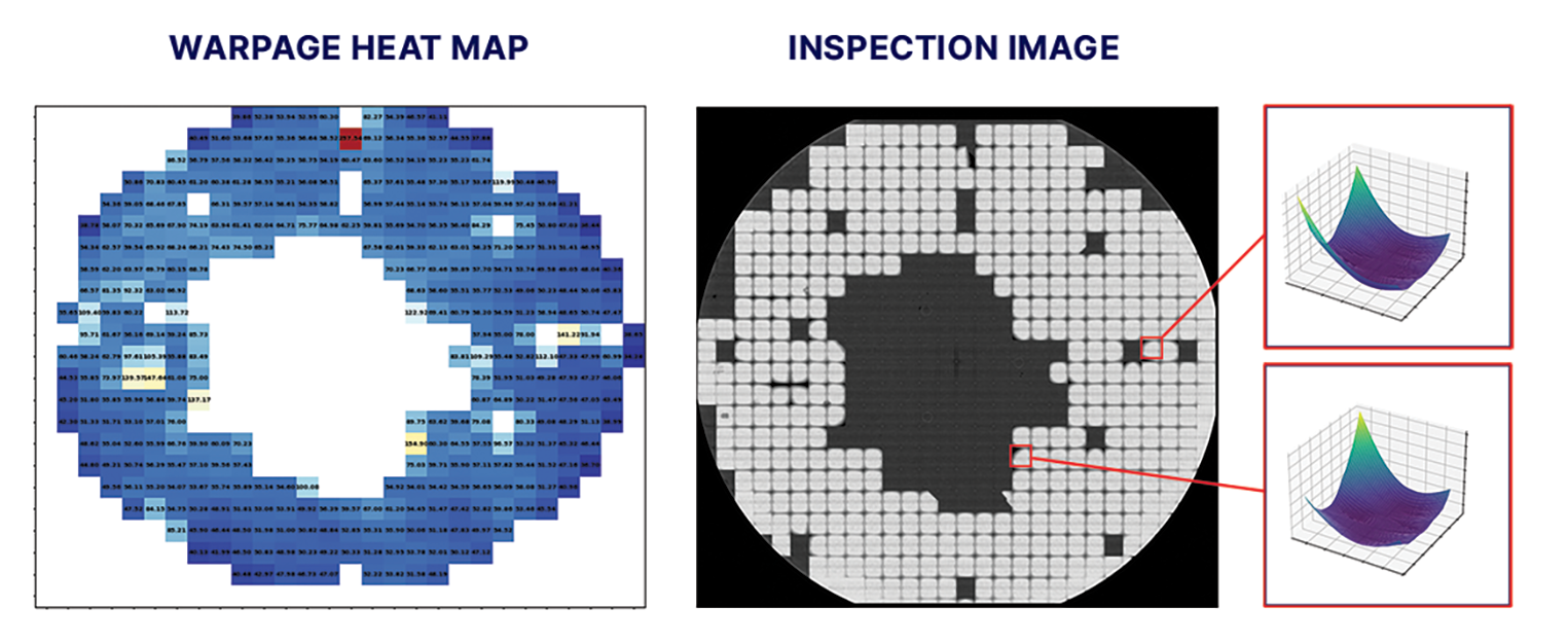
With the number of layers in an HBM stack continuing to rise, addressing die warpage becomes even more essential (Figure 2). First of all, die warpage significantly compromises stack alignment and bonding quality. This is especially critical given the extremely tight tolerances of HBM. In addition, warpage can also result in voids, opens, and a host of other issues leading to electrical failures, mechanical stress and cracking, yield loss, and thermal performance degradation, resulting in overheating and reduced performance. Meanwhile, organic residue can result in surface contamination, voids and delamination, oxidation and corrosion, and diminished yield and reliability.
Properly identifying cracks and alignment errors in bumps poses another challenge (Figure 3). Cracks often occur during the dicing and backside grinding process and can break the electrical path, leading to open circuits. They often propagate due to thermal cycling, especially in materials with different coefficients of thermal expansion (CTE), weakening the bump structure. Even if initially functional, cracked bumps are prone to failure under thermal or mechanical stress during operation.
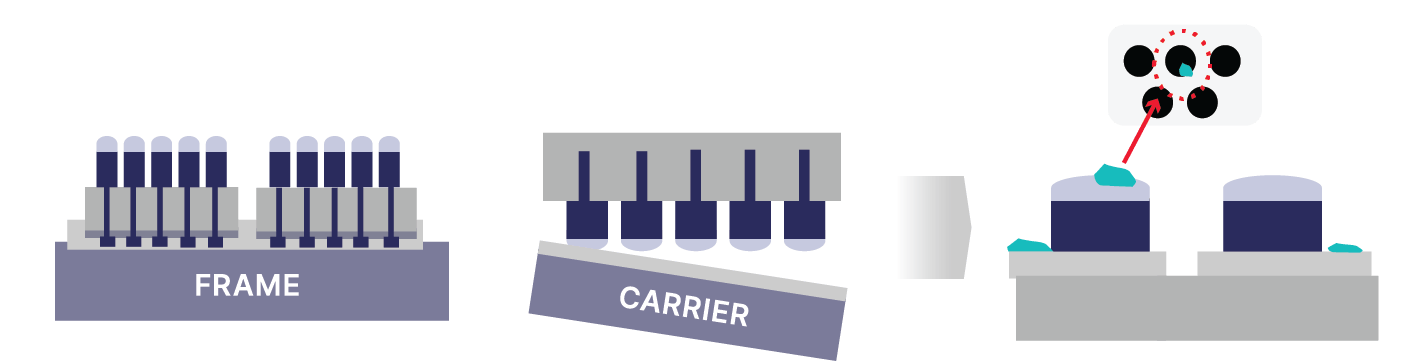
Misalignment of dies is another problem. It is often caused during the pick and place step due to the lack of backside patterns. This lack of patterning makes it difficult to tell if overlay is accurate—this is something with which automated optical inspection systems struggle.
Rise of hybrid bonding
The key reason hybrid bonding has emerged as a new technology for HBM is simple: improved interconnect density and smaller package sizes. To begin with, hybrid bonding enables finer interconnect pitches, less than 10μm, allowing for more I/O terminals in a smaller area. This increased density translates directly into higher bandwidth and improved overall performance.
Traditional bump-based stacking introduces gaps of about 30μm between dies. Hybrid bonding offers direct Cu-to-Cu connections, thereby achieving near-zero spacing between dies, significantly reducing overall package thickness and offering lower resistance and better thermal conductivity than bump-based methods. This improves signal integrity, reduces power consumption, and enhances heat dissipation, all of which are critical for HBM.
Finally, hybrid bonding supports several configurations: wafer-to-wafer, die-to-wafer, and die-to-die, offering flexibility in manufacturing and integration. This adaptability is vital for scaling HBM technologies across different applications and performance tiers.
With our introduction to bumps and hybrid bonding complete, we now turn to a comparative discussion of these two technologies, building on earlier points and exploring new ones.
Bump vs. hybrid bonding
Bumps have several advantages over hybrid bonding. As a mature technology, they are widely used and well understood in the industry, are compatible with existing flip-chip and underfill processes, and are scalable for moderate density. The cost of bump technologies is lower than hybrid bonding technologies. Bumps, however, have a number of disadvantages compared to hybrid bonding. The most significant of which are the pitch limitations of bump technologies, which struggle at pitches below 10µm due to challenges in plating uniformity and solder reflow. Bumps also require underfill, which can introduce stress and complicate thermal management.
Despite the limitations noted above, bump technology continues to evolve. Leading suppliers of bump plating systems project a continued downscaling of bump dimensions, with diameters decreasing to the 4µm-5µm range and heights dropping as low as 1µm to 2µm. At a 10µm pitch, the lateral footprint remains sufficient to support the high-density I/O requirements of advanced memory architectures. Concurrently, the reduced bump height enables vertical integration of up to 16 stacked HBM dies within the 775µm maximum package height defined by Joint Electron Device Engineering Council (JEDEC) standards. Consequently, bump interconnects remain a viable and scalable solution for next-generation HBM, and major manufacturers are maintaining substantial R&D investments in bump technology.
Hybrid bonding, while promising, presents its own set of challenges. In addition to being more expensive than traditional bump technologies, hybrid bonding may require manufacturers switching from bump technology to purchase new equipment and adopt new process flows. In addition, hybrid bonding is especially sensitive to particles and organic residues; for example, even 1µm particles can cause defects. Such residues can prevent proper contact, trap gases or moisture, and lead to void formation during bonding. These voids can cause delamination or incomplete bonding, reducing mechanical integrity and electrical continuity.
Interconnect solutions
Process control for hybrid bonding is challenging, but these obstacles can be addressed by employing a suite of advanced metrology and inspection technologies, as well as analytic software solutions.
High-speed, sub-micron inspection can be used to detect surface anomalies such as particles, residues, and backside and edge defects (Figure 4). This ensures that bonding surfaces are clean and defect-free before the bonding process begins. As for overlay misalignment, the capability to measure wafer topography and alignment with sub-micron precision enables accurate die placement and reduces the risk of misalignment during bonding. As for voids, a non-contact, immersion-free acoustic metrology technology capable of detecting voids down to 1µm is effective at identifying bonding defects that could lead to electrical or thermal failures. Furthermore, a sub-micron inspection system can be used to detect defects like cracks and delamination caused by thermal or mechanical stress.
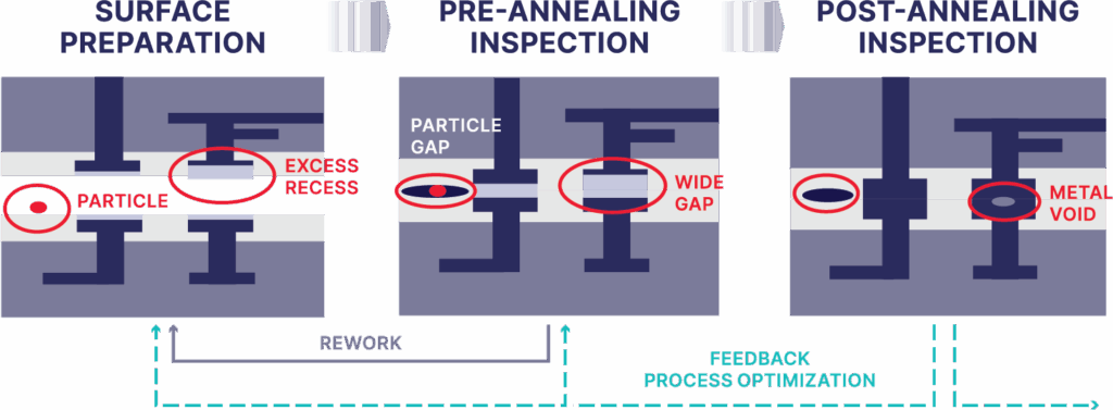
Figure 4: Hybrid bonding metrology and inspection challenges.
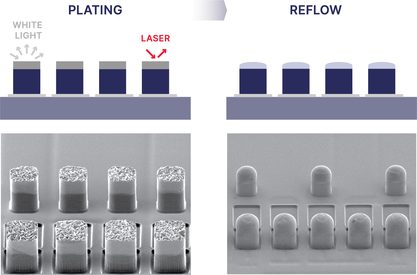
In the case of bump-based interconnects, the ability to measure Cu-to-Cu bump height down to 1.5μm will be key. However, several of today’s technologies employ white light illumination technologies that are unable to properly identify defects on these exceptionally small Cu pillars before reflow (Figure 5). After reflow, the bump shape is very clean and very smooth; but before reflow and after plating, the Cu is very rough. Typically, when white light hits a very rough surface, the light randomly scatters. However, an inspection system that uses a coherent wavelength laser technology can overcome this challenge.
In addition to the points noted above, an integrated system using analytical software can be used to detect errors and provide real-time defect analysis and statistical process control. Software can be used to provide in-line process control insights about defects and offer actionable corrections and is capable of handling millions of bumps per wafer, with each bump generating multiple data points. This integration helps manufacturers trace contamination sources and optimize cleaning steps, improving bonding reliability.
Summary
New technologies are actively being adopted for interconnect control in HBM. In the case of bump process control, the sector is moving toward smaller dimensions, 12µm to 4µm in high-volume manufacturing and below 2µm in R&D. Meanwhile, hybrid bonding is gaining traction due to its ability to support higher interconnect density and performance. This shift is driving the adoption of advanced inspection and metrology techniques, including an opto-acoustic void detection technology capable of detecting voids down to 1µm—a critical point for yield in HBM production.
Foundries are integrating bump inspection and metrology tools into their advanced packaging lines, especially for custom HBM and logic solutions. At the same time, hybrid bonding adoption is accelerating, particularly in the case of chiplet-based and heterogeneous integration strategies.
This year, R&D is expected to push microbump pitch to 6µm and hybrid bonding density to 60 interconnects/mm². In the coming years, microbump pitch may scale down to 3µm, while hybrid bonding density could reach 100 interconnects/mm². Long term, hybrid bonding is projected to become a mainstream interconnect technology, surpassing microbumps in many advanced applications, with densities reaching 150 interconnects/mm² and microbump pitch shrinking to 1.5µm.
As it stands today, there is no single solution for all HBM use cases. Instead, manufacturers may adopt an approach leveraging both bump and hybrid bonding, supported by a comprehensive process control strategy that integrates metrology, inspection, and advanced analytics.
Biographies
Damon Tsai is the Senior Director of Product Marketing, Inspection, at Onto Innovation, Milpitas, California. He joined the company in 2018 and has extensive experience in inspection and metrology, with a specialized focus on semiconductor FEOL, advanced packaging, OSAT, and specialty markets like RF, Power, and CIS.
Woo Young Han is Product Marketing Director, Inspection, at Onto Innovation, Richardson, Texas. He joined Onto Innovation in 2000 and holds an Electrical Engineering degree from the University of Toronto.
You Have a Challenge? Let’s talk.
We’d love to connect with you.
Looking to learn more about our innovative solutions and capabilities? Our team of experts is ready to assist you. Reach out today and let’s starts a conversation about how we can help you achieve your goals.
Let’s Talk
"*" indicates required fields
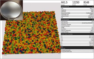
Optical measurement technology delivers nanometer resolution for real-time roughness analysis.
Surface roughness is the deviation of a surface from its ideal form. The larger the deviation, the rougher the surface. When using a 2D measurement technique, the roughness average is represented as Ra, while it is known as Sa when calculating roughness from 3D area measurements.
Most machined surfaces have an average roughness (Sa) of 200 nanometers (nm) to 2 µm (8 to 80 µin but can go down to less than 25nm. Traditionally, surface roughness has been measured using either subjective visual tests or two-dimensional (2D) stylus tools. For aerospace components, deviations from surface roughness specifications can cause performance issues such as increased wear, fracturing, disrupted fluid or air flow, poor adhesion of coatings and lubricants, and reduced corrosion resistance.
While visual testing techniques are inexpensive and easy to use, they do not deliver quantitative results. They cannot meet the gage repeatability standards many aerospace manufacturers require.
Using a 2D stylus offers quantifiable results, but faces hurdles in meeting gage repeatability standards, especially on the shop floor. The 2D stylus offers only a single trace with limited data points, and the results are directionally dependent-based on whether the scan is performed horizontally, vertically, or at an angle across the sample surface. Measuring corners and odd angles adds further challenges. The resolution of a 2D stylus system also depends on the size of the stylus tip.
Additionally, a 2D stylus is a contact-based tool. It can be damaged when measuring parts, especially at the edges, and can potentially damage the part itself.
Traditional quality control lab 3D optical profilers offer many advantages over 2D tools, including higher resolution, a larger measurement area of 3D data, and a true 3D Sa value. But they are limited by long turnaround times and the need to replicate large parts that do not fit under the microscope. They are also vibration-sensitive and require stable platforms, making them impractical for shop-floors.
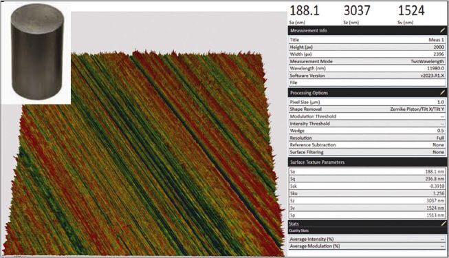
The 4Di InSpec SR, addresses these challenges with a portable 3D surface gauge that delivers microscope-quality nanometer resolution measurements in real time. With a field of view of 1mm x 0.8mm, the measurement system acquires millions of data points in a single area, with a roughness accuracy of u0026lt;0.5%, and can measure machined surfaces from mirror-smooth to sandpaper-rough.rnrnThe system enables in situ surface finish and roughness measurements below 25 nanometers in seconds, while meeting gage repeatability standards. Machinists can achieve surface finishes at very small scales, creating performance improvements whether the part is a turbine blade or rivet on a wing.
The 4Di InSpec SR measures roughness on large components without the need for replication by bringing the system directly to the part. Its scratch-free optical technology eliminates surface damage concerns. The system employs vibration-immune technology, enabling fast quantification of surface roughness for both smooth and rough components on the shop floor.
A significant capability of the 4Di InSpec SR is its robot compatibility for automated measurements. Looking to the future, there are numerous opportunities to extend its benefits in shop floor applications, including automation integration, multi-sensor systems for macro and micro level measurements, and advanced predictive analytics capabilities.
The 4Di InSpec SR represents a significant advancement in quality control technology, offering aerospace manufacturers a unique real-time, shop floor surface measurement solution that bridges the gap between traditional laboratory precision and production-line practicality.