

Abstract
In this review we discuss two recent CnCV metrology advancements, namely: 1. enhancement of throughput and 2. use of electrical defect mapping for yield prediction. Novel 10x faster measurements of critical WBG semiconductor electrical parameters are based on the discovery of a linear UV radiation induced electrical charge biasing. Example results for an AlGaN/GaN HEMT structure illustrate wafer uniformity mapping reduced from hours to minutes and enabling the prediction of the useful wafer area. The second development on SiC device yield was realized as a joint project with Nexperia and Fraunhofer IISB in Germany [2]. The project took advantage of the unique electrical defect mapping capability of the QUAD (Quality, Uniformity and Defect) technique in CnCV tools. Macro and micro-scale QUAD mapping applied to a merged PiN Schottky (MPS) diode manufacturing process correlated QUAD bin map results with failed dies identifying the culprit epi-layer and process induced defects. This development paves a realistic path for meeting the demand for more advanced electrical defect detection and improving device yield prediction.

You Have a Challenge? Let’s talk.
We’d love to connect with you.
Looking to learn more about our innovative solutions and capabilities? Our team of experts is ready to assist you. Reach out today and let’s starts a conversation about how we can help you achieve your goals.
Let’s Talk
"*" indicates required fields
Specialty devices are the unsung heroes of modern life. For many in the semiconductor industry today, the spotlight is on the SiC and GaN power devices used in automotive, green energy, fast-charge consumer electronics (CE), and high-performance computing (HPC) applications (Figures 1 and 2).
However, specialty devices are more than just power devices. They are a broad class of semiconductor components delivering a variety of functions across multiple industry segments, including microelectromechanical systems (MEMS) in automobiles and CE to radio frequency (RF) filters for 5G/6G communications.

Figure1: Planar SiC MOSFET and trench SiC MOSFET

Figure 2: Vertical GaN and GaN on Si high electron mobility transistor (HEMT)
Photonics are another type of specialty device making industry waves. Previously viewed as something of a dark horse in the specialty sphere, photonics have made a comeback. Today, photonics are being used for 3D sensing in multiple CE applications such as smartphone user verification and 3D imaging, automotive applications in which scanning lasers are used in advanced driver assistance systems (ADAS); and telecommunications applications where photonics have long been used as optical transceivers supporting the conversion of copper wiring to optical fiber communications in data centers. While these applications and others exist for photonics, the killer photonics application is shaping up to be co-packaged optics (CPO), which enables optical communications directly from packaged XPU devices supporting AI applications.
When it comes to the broad category of specialty devices, nearly all of them are either manufactured on or previously manufactured on 150mm or 200mm wafers. However, specialty devices are moving to larger wafer sizes, either 200mm or 300mm depending on device type.
With many specialty devices scaling to larger wafer sizes, the semiconductor industry faces new challenges in process control. After all, specialty devices are known for delivering specialized features or capabilities based on a unique process step or material that often requires a customized inspection and metrology solution.
To optimize the manufacturing process, real-time process control —powered by data analytics and software —has become an indispensable requirement in specialty device fabrication. To scale specialty technologies for high-volume manufacturing, manufacturers need integrated solutions and specialty-focused platforms offering flexibility, precision, and automation across multiple wafer sizes.
In this three-part blog series, we will begin by discussing one of the most important trends in specialty devices, the transition to larger wafer sizes and what this means for specific devices. The following blogs will focus on the challenges facing the manufacturing of specialty devices and the solutions addressing these challenges.
From Niche Applications to Mainstream Products
Originally, specialty devices were referred to as More-than-Moore devices because the use of these devices went beyond the simple node scaling of traditional CMOS devices. They also were being enabled by one or more “specialty” materials or process steps. In fact, the semiconductor industry did not start using the term “specialty devices” until these devices transitioned from niche applications to mainstream products and high-volume production.
But what exactly are the benefits of these specialty materials? Let’s consider the case of specialty power devices.
The compound semiconductors used in power specialty devices, SiC and GaN, can handle high voltages more efficiently than traditional Si. They provide the ability to switch high voltages in increasingly smaller areas and at higher speeds than their silicon-based counterparts. They do this without the elaborate cooling that would otherwise be required. As these materials scale to larger wafer sizes, they necessitate upgrades in wafer fabrication equipment, inspection, and metrology tools.
Transitioning Wafer Sizes
Specialty devices have long been the domain of 150mm and 200mm wafers, with CMOS image sensors (CIS) and power management devices being the exception. That’s all changing.
On the compound semiconductor front, the high demand for GaN-based high-power, fast-switching technologies is motivating a wafer size transition from 200mm to 300mm while SiC power devices are transitioning from 150mm to 200mm in high-volume manufacturing. In addition, photonics technologies now span wafer sizes of 150mm to 300mm, and MEMS devices are offered at 300mm.
As more specialty device technologies move into high-volume manufacturing, we can expect to see a greater demand for 300mm silicon, glass, and compound semiconductor-based wafer applications. However, this transition to larger wafer sizes introduces unique challenges for each specialty device type. These devices and their challenges include:
MEMS: Larger substrates and diverse materials (Si, glass, thick metals) require tighter process control of etch depth and CD, feature height across bowed or warped wafers, and surface roughness.
SiC Power: As SiC power moves to 200mm, inspection and metrology must expand sampling, deal with increased crystal defects, and support device architecture transitions profiling complex trench MOSFETs (e.g., top/bottom CD) without killing throughput. Insufficient sampling on larger wafers creates blind spots that hurt yield and cost of ownership.
GaN Power: Moving GaN to 300mm wafers increases within-wafer variation, requiring more measurement points and precise control of trench/HEMT critical dimensions to maintain uniform performance, while dealing with increasingly brittle and bowed or warped materials.
Photonics and CPO: Co-packaged optics require metrology tools designed for die-to-die and wafer bonding (voids, Cu dishing, film variation), sub‑micron alignment, and warpage, which affects optical coupling on larger wafers and multi‑die assemblies.
CIS: CIS stacks drive high sampling density for overlay and CD uniformity. These stacks require integrated chemical mechanical planarization metrology and analytical tools to catch excursions quickly as die counts and wafer diameters increase.
To meet these challenges and others, manufacturers need upgraded metrology and inspection tools, many of which will come from suppliers with a long-standing relationship with specialty technologies. These suppliers are best prepared to meet the wafer handling, on-wafer materials, and cost-of-ownership requirements that have become synonymous with the specialty device markets.
Conclusion
The emergence of specialty devices as a vibrant market of their own is driven by the increasing complexity and functionality of end products. Even in mature markets, such as smartphone and automotive, manufacturers continue to innovate by adding new features, which, in turn, fuels demand for additional specialty devices.
In our next blog, we will further explore the many challenges facing each type of specialty device. We hope you join us as we discuss those challenges and, in part three of our series, the solutions that are available in the specialty space today.
Christopher Haire is a marketing content specialist at Onto Innovation and a former business journalist.
You Have a Challenge? Let’s talk.
We’d love to connect with you.
Looking to learn more about our innovative solutions and capabilities? Our team of experts is ready to assist you. Reach out today and let’s starts a conversation about how we can help you achieve your goals.
Let’s Talk
"*" indicates required fields
Mid-infrared ellipsometry offers a powerful approach for non-destructive optical critical dimension (OCD) metrology in advanced semiconductor manufacturing. This technique supports in-line measurements of high aspect ratio structures, such as those found in 3D NAND memory devices. The incorporation of quantum cascade lasers and fast phase modulation allows rapid acquisition of Mueller matrix elements with high spatial resolution and sub- Å precision. Material-specific absorption in the mid-infrared range allows depth-resolved profiling of device structures, overcoming the limitations of conventional OCD. Rigorous coupled wave analysis is used to extract structural parameters from the measured spectra. Agreement with destructive reference metrology has been demonstrated on a variety of structures. The ability to measure multiple Mueller elements further enhances characterization of complex geometries, making mid-infrared ellipsometry a valuable tool for process control in semiconductor fabrication.
This article may be downloaded for personal use only. Any other use requires prior permission of the author and AIP Publishing. This article appeared in Journal of Applied Physics (Vol.139, Issue 7) and may be found at https://doi.org/10.1063/5.0310009
DOI: 10.1063/5.0310009
You Have a Challenge? Let’s talk.
We’d love to connect with you.
Looking to learn more about our innovative solutions and capabilities? Our team of experts is ready to assist you. Reach out today and let’s starts a conversation about how we can help you achieve your goals.
Let’s Talk
"*" indicates required fields
AI workloads are pushing the boundaries of compute, memory, and interconnect architectures, and to meet these goals, manufacturers are rapidly accelerating advanced logic and DRAM development. Chief among these innovations: gate-all-around (GAA) logic transistor and vertical gate (VG) DRAM, two device architectures that promise higher performance, improved power efficiency, and greater scalability.
However, the arrival of these device architectures introduces new levels of manufacturing complexity brought on by increasing high aspect ratios (HAR) and the continued shrinking of device dimensions by roughly 20–30% per generation. Fortunately, new capabilities in optical critical dimension (OCD) metrology are up to the challenge of measuring and monitoring features, such as gate profiles, film thickness, and structural uniformity, at the nanometer scale. With the right tools on hand, manufacturers can maintain high volume process control for GAA logic and VG DRAM in the AI era (Figure 1).
Figure 1: GAA (left) and vertical gate DRAM (right) present new challenges for process control (pictured above)
These new capabilities are enabling the delivery of accurate, high throughput measurements across complex 3D geometries like GAA and VG DRAM by offering smaller spot size, higher signal sensitivity, and enhanced precision.
But before we discuss these new capabilities, let’s dive deeper into the challenges of both device architectures. We’ll start with GAA.
Challenges and Solutions
GAA transistors feature HAR channels and stacks of multi-layered nanosheets, in some cases as thin as 10nm. The manufacturing complexity lies in controlling individual nanowires and accurately characterizing buried nanowires within three-dimensional architectures. Precise control over nanowire dimensions is critical for achieving the desired electrical performance, including higher transistor speeds and lower power consumption. As such, GAA manufacturers need metrology solutions capable of extracting unique signals with high sensitivity and precision from each layer, even those deeply buried under semi-opaque stacks.
While GAA logic presents unique challenges in transistor scaling, VG DRAM introduces equally complex demands in memory architecture. VG DRAM involves vertical nanowire etch, multi-layer ultra-thin film deposition, sidewall trim, and buried bitlines, electrical connections that are embedded deep within the silicon substrate rather than being placed on the surface, helping reduce the footprint of each memory cell. Additionally, VG DRAM for HBM4 features smaller cell blocks. Addressing these challenges requires an OCD system with a significantly smaller spot size in order to conduct direct on-device measurements. This, unfortunately, reduces the signal strength of optical systems.
For both GAA logic and VG DRAM devices, incorporating real-time stabilization technologies and advanced optical modeling can improve measurement precision and enable tighter process windows. In addition, AI-guided analysis allows fabs to create robust measurement recipes faster and with greater accuracy for highly complex device structures like nanosheets and VG DRAM cells. Analysis software also enables more accurate measurements that are scalable across multiple tools, while supporting smart manufacturing and predictive analytics for advanced AI applications.
Many of today’s OCD metrology tools, however, have limited SNR to measure these increasingly smaller changes in the complex device structure, while other systems do not have sufficient information to separate signals from multiple parameters (e.g., dimensions from individual nanowires) in complex device structures. Furthermore, most OCD metrology systems feature large spot sizes that do not fit into the reduced DRAM cell block area for HBM4.
Without the proper advanced metrology solutions addressing these challenges, manufacturers risk variability in critical dimensions and compromising device performance and yield. As such, more data channels and enhanced SNR at higher speed are needed to overcome the reduced signal strength due to smaller geometries and increased signal complexity from higher nanowire stacks.
Onto Innovation has recently added a number of optical and algorithm innovations to its OCD arsenal, such as new multi-polarization angle data channels with real-time stabilization technologies to enhance information content and SNR. These new capabilities offer advanced optical modeling, improving measurement precision, and robustness. Furthermore, the addition of AI-guided analysis software allows fabs to create robust measurement recipes faster and with greater accuracy for highly complex device structures. This includes nanosheets and VG DRAM cells. The use of analytical software also enables more accurate measurements and is scalable across multiple tools, all in support of smart manufacturing and predictive analytics for advanced AI applications.
Conclusion
As the semiconductor industry advances toward AI-optimized architectures, the need for more precise and adaptive process control has become critical. The new OCD capabilities discussed in this blog enable tighter control over individual nanowires in GAA logic and allow for more accurate measurements within increasingly compact VG DRAM cell blocks. Combined, these innovations represent a foundational shift in how the industry measures, monitors, and optimizes the most advanced semiconductor technologies.
Jiangtao Hu is a product marketing senior director at Onto Innovation.
You Have a Challenge? Let’s talk.
We’d love to connect with you.
Looking to learn more about our innovative solutions and capabilities? Our team of experts is ready to assist you. Reach out today and let’s starts a conversation about how we can help you achieve your goals.
Let’s Talk
"*" indicates required fields
Onto Innovation with LPKF Laser & Electronics SE
The drive for increased performance is enticing some advanced packaging manufacturers to transition from traditional organic substrates to glass core substrates, a switch that comes with numerous benefits. Compared to organic substrates, glass core offers superior mechanical strength, is better suited for large package sizes, provides improved electrical properties, and has the ability to meet new line/space requirements of 1.5µm and below in support of the dense interconnects for advanced logic nodes and high-performance packages.
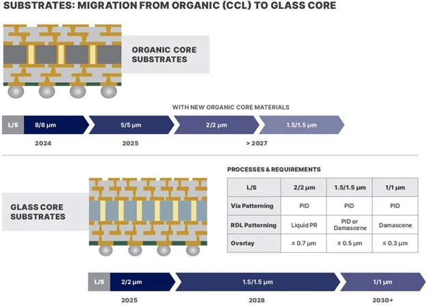
Figure 1: Roadmap for organic and glass core substrates
Glass substrates, however, are not immediately poised to push aside organic substrates as the preferred material for advanced packaging substrates. Thanks to a host of innovations, organic substrates will remain viable for advanced packages. Regardless, many manufacturers are developing glass substrates now instead of waiting for organic substrates to reach their line/space endpoints.
To optimize this transition from organic to glass substrate, interconnect technologies are changing as well.
Through glass vias (TGVs) are the critical vertical electrical connections that pass through a glass substrate. They require ultra-precise processing, which leads to several obstacles which must be overcome. Glass is brittle, after all, and this creates handling challenges, along with many other potential issues across the fabrication process. Each step—from laser modification on the panel to wet etching, metallization and planarization—opens the process to a host of potential errors, including cracks, critical dimension variation, incomplete debris removal, voids, overfill, and over-polishing (Figure 2). Cracks, in particular, are problematic. A small crack early in the process has the potential to grow into a much larger, potentially “killer” defect later and affect the performance and reliability of the end product.
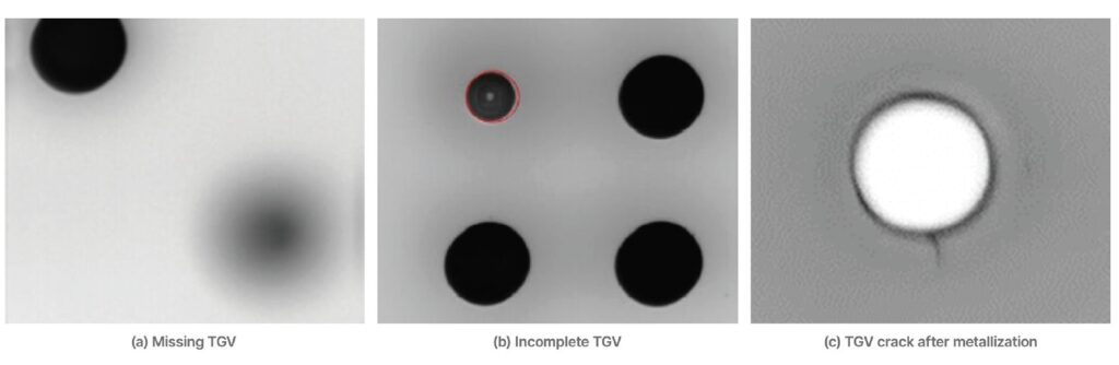
Figure 2. TGV Defect Examples (a) Missing TGV, (b) Incomplete TGV, (c) TGV crack after metallization.
These TGV process control challenges are not limited to cracks. The position accuracy of TGVs is vital for reliable electrical connections between the front and back of the glass substrate. Even slight misalignments can lead to signal integrity issues or device failure. In addition, the shape and size of the vias is another area of concern; as a result, the critical dimensions (CD) of these vias must be tightly controlled. The relationship between the top, bottom, and waist diameters of a TGV determines the profile of the via. Moreover, if the sidewall is too steep or reentrant (narrower at the bottom), it can affect the plating process, leading to incomplete metal-filled vias or voids, impacting the electrical signal performance and reliability of the final device.
Today, manufacturers are adopting a number of best practices to optimize the TGV process. On the incoming quality control front, proper process control includes identifying any defects on the surface or in the bulk of the incoming glass substrate and determining the thickness uniformity of the glass. Following each step in the TGV fabrication process, measuring critical dimensions after each process step is of imminent concern. Controlling for each of these is critical to maintaining the integrity of the final product and optimizing yields.

Figure 3: The TGV development process
In this article we will detail the entire TGV manufacturing process, starting from a bare glass panel and moving on to the fabrication of the via, TGV Cu plating, and TGV chemical mechanical planarization (Figure 3). As we discuss the process, we also will address the challenges manufacturers face at each step and expand on a unique ultra-fast laser drilling technique called laser-induced deep etching (LIDE®) that is used in the creation of vias. Afterward, we will move onto the process control solutions that enable manufacturers to reach and maintain high volume production.
TGV Manufacturing: Every Step Counts
The manufacturing of TGVs begins with a defect-free glass panel. Defects in an incoming glass panel will only compound as the TGV process moves forward. Even microscopic defects such as cracks, inclusions, scratches or surface particles can develop during manufacturing, leading to catastrophic failures. In addition, photoresist coating defects, monolayer organic residues, and variations in coating thickness can also lead to serious process control complications. Each of these issues are especially problematic in TGV manufacturing where precision and structural integrity are paramount.
Furthermore, thickness uniformity across the glass panel is key. Non-uniform thickness in a glass core substrate can significantly impact the fabrication and reliability of TGVs. As the thickness of the glass varies, the depth control during the via formation can become inconsistent, leading to incomplete or over-etched vias, increasing, for example, the variation of the waist diameter and affecting the performance of the final device. Another major issue: non-uniform substrates affect surface planarity, which is crucial for subsequent fabrication steps such as photolithography, solder bumping, and die bonding.
Following these steps, the panels undergo thorough cleaning using wet chemical and plasma-based methods to remove surface contaminants. However, this step presents several challenges. Particulate contamination, if not fully eliminated, can affect laser modification or interfere with the adhesion of subsequent layers. Additionally, any residual surface roughness can negatively impact downstream processes such as lithography and metallization, potentially compromising the fidelity of fine features.
The next step is the via formation stage. Various glass processing techniques have been used in the industry, including mechanical drilling, direct laser ablation, and lithography-based techniques with photosensitive glass followed by isotropic wet etching or deep reactive-ion etching (DRIE). A novel hybrid process utilizing laser exposure and selective wet chemical etching has been developed by LPKF Laser and Electronics SE: laser induced deep etching (LIDE).
Understanding the LIDE Technique for Via Formation
The LIDE technique is a two-step fabrication method designed to enable the high volume manufacturing of glass substrates for advanced semiconductor packaging through a combination of laser modification and selective wet chemical etching.
First, an ultrashort-pulsed laser is focused into the bulk of the glass, inducing a non-ablative modification of the material’s chemical and physical properties along a defined path. This highly localized modification, typically less than 3µm wide, spans the full thickness of the glass without removing material or introducing microcracks, thermal stress, or debris. Next, the glass panel is immersed in a chemical etchant, such as hydrofluoric acid or a hot alkaline solution. The laser-modified regions etch up to 100 times faster than the unmodified glass, enabling the formation of deep, narrow vias with smooth sidewalls and minimal tapering.
This approach allows for precise TGV formation with minimal particulate generation, no heat-affected zones, and highly uniform diameters (Figure 4). By avoiding melt ejection and suppressing microcracks, the technique helps to ensure mechanical integrity and cleanliness.
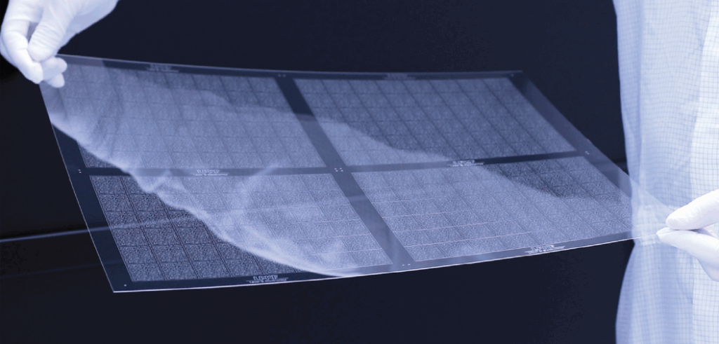
Figure 4. Glass panel with TGV. (Source: LPKF)
Post-via Processing: The Next Critical Steps
Following via formation, the substrate undergoes cleaning and surface conditioning. This includes wet chemical etching and plasma treatments to remove debris and prepare the surface for metallization. This step must be finely tuned to avoid thermal damage. Common challenges include managing heat input and debris ejection. Potential defects include microcracks from thermal stress and irregular via profiles complicating downstream metal deposition. Furthermore, the incomplete removal of debris can result in voids during the plating process, compromising the integrity of the via fill, while over-etching can damage the via walls or reduce the adhesion of subsequent layers, both of which can lead to reliability issues in the final device.
The seed layer deposition step follows. In this step a thin conductive layer, commonly Ti/Cu or Cr/Cu, is applied using sputtering or electroless plating. This layer serves as the foundation for electroplating. Challenges at this stage include achieving uniform coverage inside the high-aspect-ratio vias, which is critical for ensuring complete and reliable Cu fill. Poor surface preparation or contamination can also lead to adhesion failures, which may manifest as delamination or electrical discontinuities during device operation.
Via filling is then performed using electroplating to deposit Cu into the vias. This step must be carefully controlled to avoid common defects such as voids or seams within the Cu fill, which can compromise electrical conductivity and mechanical strength. Overplating is another concern, as it can create surface topography issues that complicate subsequent planarization and patterning steps.
Once the vias are filled, surface planarization is carried out using chemical mechanical polishing (CMP). This step removes excess Cu and the seed layer to create a flat surface. However, CMP can introduce its own set of challenges. Excessive dishing or erosion of Cu features may occur, especially if the process is not uniform across the panel. Non-uniform planarization can lead to variations in layer thickness, which may affect the performance and reliability of the final device.
Redistribution layer (RDL) formation follows. This involves photolithography, metal deposition, and etching to create the necessary interconnect patterns on the sides of the glass core. This step is highly sensitive to alignment and patterning accuracy. Misalignment with the underlying vias can result in open circuits or shorts, while defects in the patterning process can lead to electrical failures or reduced yield.
The process nears conclusion with the final singulation of the individual dies. Residual contamination, such as ionic residues, can affect long-term reliability, especially in high-performance applications. Additionally, the brittle nature of glass makes it prone to cracking during singulation, which can result in yield loss or latent reliability issues in the field.
Process Control Solutions From Start to Finish
Before the TGV manufacturing process begins, it is important to make sure the glass panel is free of inclusion defects or cracks. A laser-based scanning and optics system designed for transparent, semi-transparent, and opaque substrates, offering sub-nanometer sensitivity and the capability of all-surface inspection, can be employed to detect surface and edge defects, including particles, scratches, pits, stains, and chips, as well as monolayer organic residues. By using multiple channel inspection modes—including polarization, slope, bright field, and dark field—manufacturers can achieve sub-nanometer inspection sensitivity. In addition to inspecting the bare glass panel, it is also important to measure the thickness of the glass before starting the TGV process. Thickness uniformity across the glass panel is key.
While inspecting the glass and measuring glass thickness before manufacturing begins is of considerable importance, there are a number of specific process steps throughout the TGV fabrication and metallization process where CD metrology and defect inspection are vital. After the TGV formation step, post-process cleaning is often required to remove debris. At this step, sub-micron automatic optical inspection is used to inspect for residual particles, microcracks, or surface anomalies that can compromise subsequent metal deposition.
Besides defect detection, manufacturers need to measure CD at the top of the via, the waist of the via, and bottom of the via, along with the via’s positional accuracy relative to the design. A high-resolution, high-throughput optical panel inspection and metrology system can be used to measure these parameters for every single TGV on the panel, enabling precise monitoring of the laser and etching process. In addition, the ability to detect alternation in laser modification, incomplete etching, microcracks along individual TGVs, larger cracks between multiple TGVs, and dimples and dents on the glass surface are crucial for process optimization.
In the metallization and planarization step, inspection systems can continue to monitor for defects such as glass cracks and residues. However, there is also an additional need for 3D metrology measurements to monitor over/under plating, excess/insufficient polishing, and surface roughness, as each of these could affect overall electrical performance. An automated inspection system with integrated 3D metrology capabilities can be the preferred all-in-one solution addressing these process control requirements.
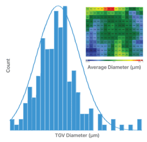
Figure 5. TGV CD distribution and analysis heat map generated by Onto Innovation’s
Discover® software.
Finally, in the inspection and yield analysis stage, the integrated use of sub-micron inspection tools and yield management software is ideally suited to support high-throughput inspection and advanced data analytics. With millions of TGVs on a panel, the ability to analyze a large quantity of inspection and metrology data within a short time period is crucial. The use of yield management software can shorten the time for analysis, identify systematic defects, and correlate process parameters with yield outcomes (Figure 5). Furthermore, manufacturers can overcome key challenges and achieve higher efficiency and yield in advanced packaging applications by automating defect classification, integrating data across systems, and enabling real-time feedback. By eliminating the need for manual review and providing consensus-based decisions, automated defect classification software can be used to enable engineers to quickly identify root causes and assess die-level quality. In addition, a robust feedback loop in which defect data is fed into analytics software allows manufacturers to make real-time process adjustments across the entire process, from the start of the process to the end.
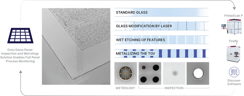
Figure 6: Full panel process monitoring includes all-surface contamination and defectivity inspection for incoming glass panel (PrimaScan™ P system) and metrology and inspection of TGVs and other defects (Firefly® system). Yield management software accelerates analysis.
Together, these solutions form a comprehensive ecosystem that supports the total TGV development process (Figure 6), enabling manufacturers to overcome key challenges and achieve higher efficiency and yield in advanced packaging applications.
Conclusion
The adoption of glass core for IC substrate is currently at the starting point of what could be considerable market growth. By 2030, glass core substrate revenue is projected to grow to $275 million, according to best case scenario results from the Yole Group. With the right tools on hand, manufacturers will be equipped to meet the rising demand for glass core substrates.
However, unlocking the full potential of glass core substrates and TGVs are not just about having tools; it is about using them in concert to build a process that is robust, repeatable, and yield optimized. As the adoption of glass as a substrate accelerates, manufacturers that invest in comprehensive process insight will be the ones that lead.
Monita Pau is Strategic and Product Marketing Director, Advanced Packaging, at Onto Innovation.
You Have a Challenge? Let’s talk.
We’d love to connect with you.
Looking to learn more about our innovative solutions and capabilities? Our team of experts is ready to assist you. Reach out today and let’s starts a conversation about how we can help you achieve your goals.
Let’s Talk
"*" indicates required fields
The demand for high bandwidth memory (HBM) is accelerating across the semiconductor industry, driven by boundary-pushing artificial intelligence, high-performance computing, and advanced graphics. These technologies require access to vast datasets, which in turn increases the need for memory solutions that combine speed, density, and power efficiency. HBM meets these demands by vertically stacking memory dies and linking them with ultra-fast interconnects.
With data rates rising, the need for increased output contact pad density is needed. To address this, bump technologies are being pushed beyond what was previously thought to be their physical and performance limits. As it stands today, some memory designers are innovating their way to bump sizes below 10µm in high volume manufacturing. Be that as may, scaling bump height to 2μm will be considerably challenging, leading some to explore hybrid bonding as an interconnect solution.
Hybrid bonding enables finer interconnect pitches of less than 10μm, allowing for more I/O terminals in a smaller area. This increased density translates directly into higher bandwidth and improved overall performance.
Traditional bump-based stacking introduces gaps of about 30μm between dies, while hybrid bonding offers direct Cu-to-Cu connections. By achieving near-zero spacing between dies, hybrid bonding significantly reduces overall package thickness and offers lower resistance and better thermal conductivity than bump-based methods. The result: improved signal integrity, reduced power consumption, and enhanced heat dissipation, each of which are critical for HBM.
Finally, hybrid bonding supports several configurations: wafer-to-wafer, die-to-wafer, and die-to-die, offering flexibility in manufacturing and integration. This adaptability is vital for scaling HBM technologies across different applications and performance tiers.
Of course, hybrid bonding offers manufacturers its own set of challenges—increased sensitivity to particles and organic residues, lower yields and introduction of more costly process and process control steps—making the decision to stick to the tried-and-true microbump technology over the emerging, innovation a debate worth having.
In this two-part blog series, we will compare these two interconnect solutions and discuss the challenges they face (Figure 1).
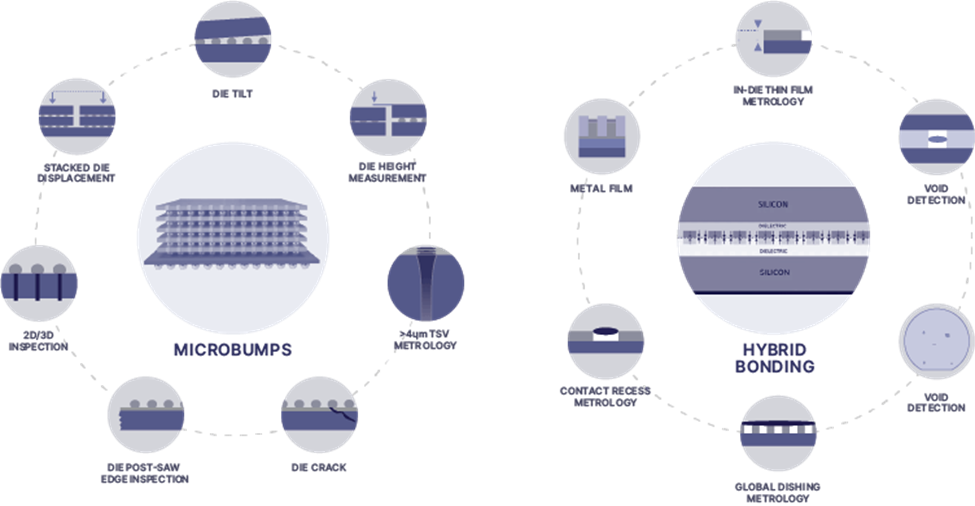
Figure 1: Interconnect challenges in microbump and hybrid bonding technologies.
Head to Head: Microbumps and Hybrid Bonding
Bumps have several advantages over hybrid bonding. As a mature technology, they are widely used and well-understood in the industry. They are also compatible with existing flip-chip and underfill processes, and are scalable for moderate density. In addition, the cost of bump technologies is lower than hybrid bonding technologies.
However, microbumps have a number of disadvantages compared to hybrid bonding. The most significant of which are the pitch limitations of bump technologies. Microbumps struggle at pitches below 10µm due to challenges in plating uniformity and solder reflow. Bumps also require underfill, which can introduce stress and complicate thermal management.
Limitations aside, bump technology continues to evolve. Leading suppliers of bump plating systems project a continued downscaling of bump dimensions, with diameters decreasing to the 5µm to 4µm range and heights dropping as low as 2µm to 1µm. At a 10µm pitch, the lateral footprint remains sufficient to support the high-density I/O requirements of advanced memory architectures. Concurrently, the reduced bump height enables vertical integration of up to 16 stacked HBM dies within the 775µm maximum package height defined by Joint Electron Device Engineering Council (JEDEC) standards. Consequently, bump interconnects remain a viable and scalable solution for next-generation HBM, and major manufacturers are maintaining substantial R&D investments in bump technology.
Hybrid bonding, while promising, presents its own set of challenges. Chief among them, hybrid bonding is especially sensitive to particles and organic residues; for example, even 1µm particles can cause defects. These residues can prevent proper contact, trap gases or moisture, and lead to void formation during bonding. Voids can cause delamination or incomplete bonding, reducing mechanical integrity and electrical continuity. Hybrid bonding also is more expensive than traditional bump technologies and may require manufacturers to purchase new equipment and adopt new process flows before moving away from bump technology.
Conclusion
As demand for HBM intensifies, the industry stands at a crossroads in interconnect technology. While microbumps have evolved to support increasingly dense and tall HBM stacks, they face several obstacles. Hybrid bonding offers a compelling alternative, but not without its own hurdles. Ultimately, both technologies are advancing in parallel, each with unique strengths and limitations.
Regardless of which interconnect technology is chosen, a comprehensive suite of interconnect solutions will be needed to address the obstacles manufacturers of HBM devices face. In the second in this two-part series, we will explore a number of these solutions that, when combined, tackle the biggest challenges facing interconnects in HBM.
Biography
Damon Tsai joined Onto Innovation in 2018 and has extensive experience in inspection and metrology, with a specialized focus on semiconductor FEOL, advanced packaging, OSAT, and specialty markets like RF, Power, and CIS. He currently serves as the Senior Director of Product Marketing, Inspection.
Woo Young Han joined Onto Innovation in 2000 and is currently Product Marketing Director, Inspection. He holds an Electrical Engineering degree from University of Toronto.
Tim Kryman is Product Marketing Senior Director, Metrology and Inspection. Tim has been with Onto Innovation for more than 20 years and holds a BS in Accounting and Information Systems from Lock Haven University and an MBA from DeSales University.
You Have a Challenge? Let’s talk.
We’d love to connect with you.
Looking to learn more about our innovative solutions and capabilities? Our team of experts is ready to assist you. Reach out today and let’s starts a conversation about how we can help you achieve your goals.
Let’s Talk
"*" indicates required fields