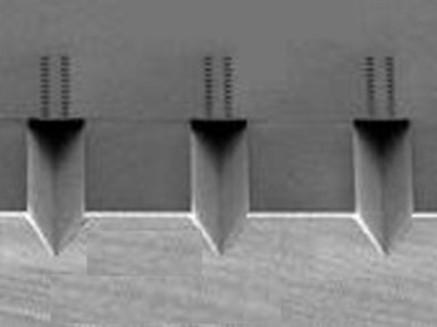

The United States is seeking to breathe new life into its domestic semiconductor packaging sector with the National Advanced Packaging Manufacturing Program (NAPMP), an initiative to “establish and accelerate domestic capacity for advanced packaging substrates and substrate materials,” according to a Commerce Department announcement from earlier this year [1]. In part, this program is the result of two very distinct trends, both of which are high-priority pursuits for governments and manufacturers. On the one hand, many nations like the U.S. are looking to shore up their semiconductor manufacturing capabilities to better protect themselves from potential geopolitical complications. Still another consideration is today’s rapidly growing demand for high-end applications like artificial intelligence (AI) and high performance computing (HPC) that are driving the need for advanced packages with 2.5 and 3D architectures. Such structures are built upon advanced integrated circuit substrates (AICS). Furthermore, the coming era of glass core substrates in advanced packaging will offer another level of challenges. The future is coming, and few want to be left behind.
Automated optical inspection (AOI) is a cornerstone in semiconductor manufacturing, assembly and testing facilities, and as such, it plays a crucial role in yield management and process control. Traditionally, AOI generates millions of defect images, all of which are manually reviewed by operators. This process is not only time-consuming but error prone due to human involvement and fatigue, which can negatively impact the quality and reliability of the review.
In the Industry 4.0 era, the integration of a deep learning-based automatic defect classification (ADC) software solution marks a significant advancement in manufacturing automation. For one, ADC solutions reduce manual workload – meaning less chance of human error and higher accuracy – and, two, they are poised to lower the costs associated with high-volume manufacturing (HVM).
Deep learning, a branch of machine learning based on artificial neural networks, is at the core of these ADC solutions. It mimics the human brain’s ability to learn and make decisions; this enables the system to recognize complex patterns in data without explicit programming. Compared to traditional methods, this approach offers a significant leap in processing efficiency and accuracy.
Onto Innovation’s Monita Pau and Prasad Bachiraju contribute to the March 2024 edition of Semiconductor Digest.
The 4Di InSpec automated metrology system (AMS) is a high-throughput, high resolution defect and feature inspection solution. The automated system can measure dozens of edge break features, chamfers, and radii in minutes rather than days, vastly improving throughput and driving down inspection costs. The 4Di InSpec AMS integrates a non-contact 4D InSpec or 4D InSpec XL surface gage with a collaborative robot and other automation for rapid production inspection. 4Di InSpec AMS systems are the turnkey option for quality control of aerospace components such as turbine blades and rotors, air foils, high pressure compressor blades, blisks, and dovetails. The high resolution gage measures in any orientation, on curved surfaces, over large and complex geometries, and in tight spaces or blind locations. The 4Di InSpec AMS instantly produces high resolution, 3D measurement results, with far more information than other methods. An inspector can immediately see both an image of the feature and easy-to-read statistics. User-friendly measurement automation software flags any out-of-spec measurements and automatically remeasures the locations.


You Have a Challenge? Let’s talk.
We’d love to connect with you.
Looking to learn more about our innovative solutions and capabilities? Our team of experts is ready to assist you. Reach out today and let’s starts a conversation about how we can help you achieve your goals.
Let’s Talk
"*" indicates required fields
Abstract
In traditional semiconductor packaging, manual defect review after automated optical inspection (AOI) is an arduous task for operators and engineers, involving review of both good and bad die. It is hard to avoid human errors when reviewing millions of defect images every day, and as a result, underkill or overkill of die can occur. Automatic defect classification (ADC) can reduce the number of defect images that need to be reviewed by operators. The ADC process can also be integrated with AOI engines to reduce nuisance defect images to reduce AOI image capturing time. This paper will focus on how to utilize Onto Innovation’s TrueADC software product to build ADC classifiers using a multi-engine (ME) solution. The software supports CNN, DNN and KNN algorithms. The use of CNN and DNN are currently mainstream in the development of deep learning (DL) for ADC classification in the semiconductor industry. We will address how to improve classification by using multiple models in the classification process with unique algorithms. As a result, the user can achieve industry requirements with very demanding specifications, like high accuracy, high purity, and high classification rate with very low escape rates.
In industries such as aircraft engines automotive, companies need to rapidly establish the quality of components, both during production and during repair and overhaul. Many of these components are highly valuable and complex, often with hundreds of features requiring inspection.
To date, much of this inspection has been completed manually—a slow and subjective process. A new, automated system is now being adopted for rapid, repeatable, non-contact measurement of features and defects on precision machined parts. Combining the flexibility of an industry-proven optical gage and
robotic automation, the system dramatically improves inspection throughput and reliability, recording quantitative data that can be tracked throughout the component’s lifetime.
You Have a Challenge? Let’s talk.
We’d love to connect with you.
Looking to learn more about our innovative solutions and capabilities? Our team of experts is ready to assist you. Reach out today and let’s starts a conversation about how we can help you achieve your goals.
Let’s Talk
"*" indicates required fields