
As demand grows for high-performance computing (HPC) and AI-driven applications, manufacturers are turning to hybrid bonding to enable the ultra-dense 3D integration required for next-generation chip architectures.
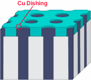
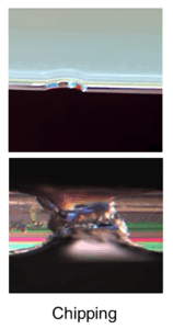
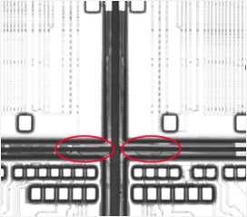
This advanced packaging technology presents significant process challenges. Surface preparation must be precisely controlled to eliminate particles, excess recess, and copper pad dishing, all of which can compromise bond quality. During pre-annealing, particle-induced gaps and wide bonding gaps can prevent proper wafer contact. Post-annealing, the formation of dielectric and metal voids introduces further risks to electrical performance and long-term reliability. If not carefully managed, these issues can lead to increased defectivity, reduced yield, and degraded performance in HPC and AI systems where reliability and speed are critical.
Source: AMD 3D V-Cache with TSMC SoIC 3D Packaging reverse engineering & costing report, Yole Group, 2022
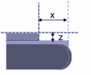
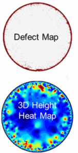
Hybrid bonding reliability starts with robust process control. Monitoring topography and detecting particles, cracks, and voids help identify defects early. Measuring copper pad dishing offers insight into surface conditions and planarity. Tight control during pre-bonding steps enables potential rework before permanent defects occur.
The following examples highlight key metrology and inspection techniques that support more consistent hybrid bonding outcomes.
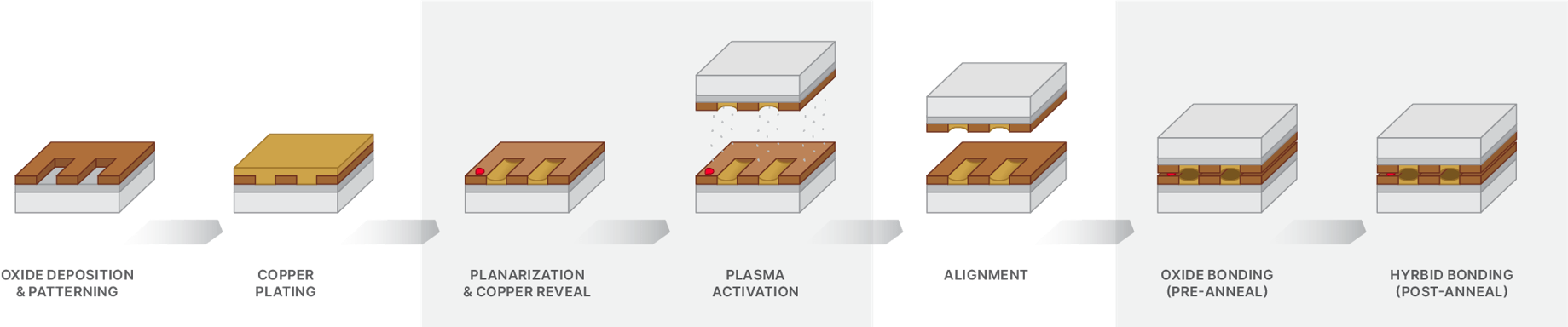
Pre-Bonding Process Control


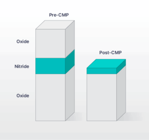
Post-Bonding Process Control
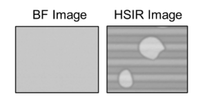
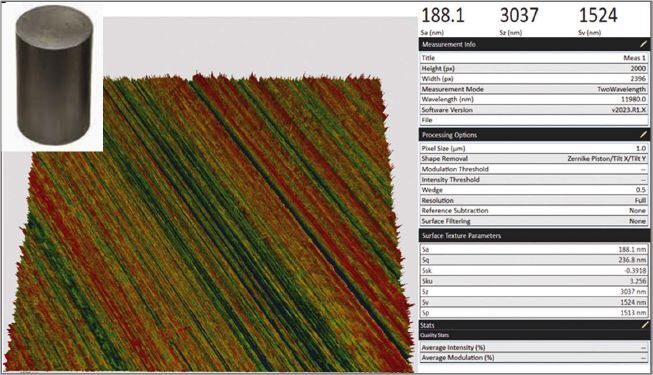
Optical measurement technology delivers nanometer resolution for real-time roughness analysis.
Surface roughness is the deviation of a surface from its ideal form. The larger the deviation, the rougher the surface. When using a 2D measurement technique, the roughness average is represented as Ra, while it is known as Sa when calculating roughness from 3D area measurements.
Most machined surfaces have an average roughness (Sa) of 200 nanometers (nm) to 2 µm (8 to 80 µin but can go down to less than 25nm. Traditionally, surface roughness has been measured using either subjective visual tests or two-dimensional (2D) stylus tools. For aerospace components, deviations from surface roughness specifications can cause performance issues such as increased wear, fracturing, disrupted fluid or air flow, poor adhesion of coatings and lubricants, and reduced corrosion resistance.
While visual testing techniques are inexpensive and easy to use, they do not deliver quantitative results. They cannot meet the gage repeatability standards many aerospace manufacturers require.
Using a 2D stylus offers quantifiable results, but faces hurdles in meeting gage repeatability standards, especially on the shop floor. The 2D stylus offers only a single trace with limited data points, and the results are directionally dependent-based on whether the scan is performed horizontally, vertically, or at an angle across the sample surface. Measuring corners and odd angles adds further challenges. The resolution of a 2D stylus system also depends on the size of the stylus tip.
Additionally, a 2D stylus is a contact-based tool. It can be damaged when measuring parts, especially at the edges, and can potentially damage the part itself.
Traditional quality control lab 3D optical profilers offer many advantages over 2D tools, including higher resolution, a larger measurement area of 3D data, and a true 3D Sa value. But they are limited by long turnaround times and the need to replicate large parts that do not fit under the microscope. They are also vibration-sensitive and require stable platforms, making them impractical for shop-floors.
The 4Di InSpec SR, addresses these challenges with a portable 3D surface gauge that delivers microscope-quality nanometer resolution measurements in real time. With a field of view of 1mm x 0.8mm, the measurement system acquires millions of data points in a single area, with a roughness accuracy of u0026lt;0.5%, and can measure machined surfaces from mirror-smooth to sandpaper-rough.rnrnThe system enables in situ surface finish and roughness measurements below 25 nanometers in seconds, while meeting gage repeatability standards. Machinists can achieve surface finishes at very small scales, creating performance improvements whether the part is a turbine blade or rivet on a wing.
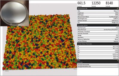
The 4Di InSpec SR measures roughness on large components without the need for replication by bringing the system directly to the part. Its scratch-free optical technology eliminates surface damage concerns. The system employs vibration-immune technology, enabling fast quantification of surface roughness for both smooth and rough components on the shop floor.
A significant capability of the 4Di InSpec SR is its robot compatibility for automated measurements. Looking to the future, there are numerous opportunities to extend its benefits in shop floor applications, including automation integration, multi-sensor systems for macro and micro level measurements, and advanced predictive analytics capabilities.
The 4Di InSpec SR represents a significant advancement in quality control technology, offering aerospace manufacturers a unique real-time, shop floor surface measurement solution that bridges the gap between traditional laboratory precision and production-line practicality.
Advanced IC substrates (AICS) have been marching toward the 2µm line/space (L/S) redistribution layer (RDL) technology node for some time (Figure 1). However, many questions remain about the ability of organic substrates to meet the line/space requirements of the next generation of advanced packages (AP), those below 2µm L/S and perhaps to 1.5µm L/S. Simply put: are organic substrates up to the challenge?
The answer to that has been no.
But with recent developments, the possibility of organic substrates reaching below 2µm appears to be changing.
Before we discuss the reasons why, we will first turn our attention to the core reasons organic substrates struggle with lower line/space requirements…
Panel-level advanced packaging technologies have been in development for more than a decade. They began as a way to reduce costs and improve yields for fan-out wafer level applications. Smartphone applications – particularly fingerprint sensors – promised the volumes that would make the investment successful.
However, memories of the fiasco of 450mm wafer efforts lived in the minds of many. Why make the investment in an ecosystem that may not demand high enough volumes to insure return on investment? Still, there were those who believed in the promise of panel-level packaging. Development efforts persevered, and PLP has moved through R&D and into pilot production. Still, through it all, many remained skeptical about there being high enough volumes to support it.
The Era of AI, coupled with the emergence of glass substrates, is set to change all that.
On September 30, 2024, I visited Onto Innovation’s headquarters in Wilmington, MA to attend the grand opening of its Packaging Applications Center of Excellence (PACE). The company has partnered with like-minded suppliers of the PLP ecosystem to accelerate the development of PLP technologies for both organic and glass substrates. These include 3D InCites Members: LPKF Laser & Electronics, Evatec, MKS-Atotech and Lam Research; as well as Resonac, Corning, and others.
The concept of zero defect manufacturing has been around for decades, arising first in the aerospace and defense industry. Since then, this manufacturing approach has been adopted by the automotive industry, and it has only grown in importance as the sector transitions to electric vehicles. Given the role semiconductors play in today’s vehicles, and will play in the future, it is no surprise the industry has adopted a zero defect approach.
However, the quest for zero defect manufacturing goes well beyond the aerospace, defense, and automotive industries. Many companies that have started or are planning digital transformations are pursuing zero defect manufacturing. Accomplishing this requires using data from a wide range of sources, including materials, products, processes, factory subsystems, and equipment. When all of this data is properly integrated, and fabs are able to take complete advantage of the analytics from their monitoring systems, the goal of a zero defect manufacturing environment is achievable.
Before we go any further, we should get one thing out of the way: zero defect manufacturing does not promise zero defects. It is a commitment to properly identifying defects and sources, giving manufacturers the opportunity to detect dormant failures early on and make proactive corrections.
Whether the discussion is about smart manufacturing or digital transformation, one of the biggest conversations in the semiconductor industry today centers on the tremendous amount of data fabs collect and how they utilize that data.
While chip makers are accumulating petabytes of data across the entire semiconductor process, a question arises: how much of that information is being fully utilized? The answer may be around 20%, according to the Semiconductor Engineering article “Too Much Fab and Test Data, Low Utilization.” Unfortunately, this poses a challenge because fab end customers are demanding highly reliable chips, in other words, chips with zero escaping defects and which offer manufacturers clear genealogy and traceability.
Many of you reading this work for companies that have started or are planning digital transformations. To do this, these companies will need to better integrate the data they collect — and that includes data from materials, products, processes, factory subsystems and equipment.
For smart manufacturing to truly live up to its potential, manufacturers will need inline automation that takes complete advantage of the analytics their monitoring systems generate, analytics which can be fed back to the process tools, manufacturing execution systems and other factory systems in real time. Working in concert, these integrated systems are essential to creating a zero defect manufacturing environment.
In the world of smart manufacturing, manufacturers will be tasked with providing timely total solutions to detect and classify defects using inspection and metrology tools, conduct root cause analysis to determine the source of said defects and, finally, employ process control and equipment monitoring using run-to-run and fault detection and classification software solutions to prevent defects from reoccurring.
In this blog, the first in our three-part series “Achieving Zero Defect Manufacturing,” we will focus on detecting and classifying defects. We will start by looking at solutions at the defect level before moving on to the die level and the wafer level.