

Through the Glass: Why the Rapid Development of TGV Demands Rigorous Analysis
Onto Innovation with LPKF Laser & Electronics SE
The drive for increased performance is enticing some advanced packaging manufacturers to transition from traditional organic substrates to glass core substrates, a switch that comes with numerous benefits. Compared to organic substrates, glass core offers superior mechanical strength, is better suited for large package sizes, provides improved electrical properties, and has the ability to meet new line/space requirements of 1.5µm and below in support of the dense interconnects for advanced logic nodes and high-performance packages.
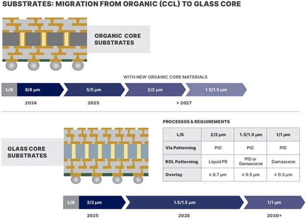
Figure 1: Roadmap for organic and glass core substrates
Glass substrates, however, are not immediately poised to push aside organic substrates as the preferred material for advanced packaging substrates. Thanks to a host of innovations, organic substrates will remain viable for advanced packages. Regardless, many manufacturers are developing glass substrates now instead of waiting for organic substrates to reach their line/space endpoints.
To optimize this transition from organic to glass substrate, interconnect technologies are changing as well.
Through glass vias (TGVs) are the critical vertical electrical connections that pass through a glass substrate. They require ultra-precise processing, which leads to several obstacles which must be overcome. Glass is brittle, after all, and this creates handling challenges, along with many other potential issues across the fabrication process. Each step—from laser modification on the panel to wet etching, metallization and planarization—opens the process to a host of potential errors, including cracks, critical dimension variation, incomplete debris removal, voids, overfill, and over-polishing (Figure 2). Cracks, in particular, are problematic. A small crack early in the process has the potential to grow into a much larger, potentially “killer” defect later and affect the performance and reliability of the end product.
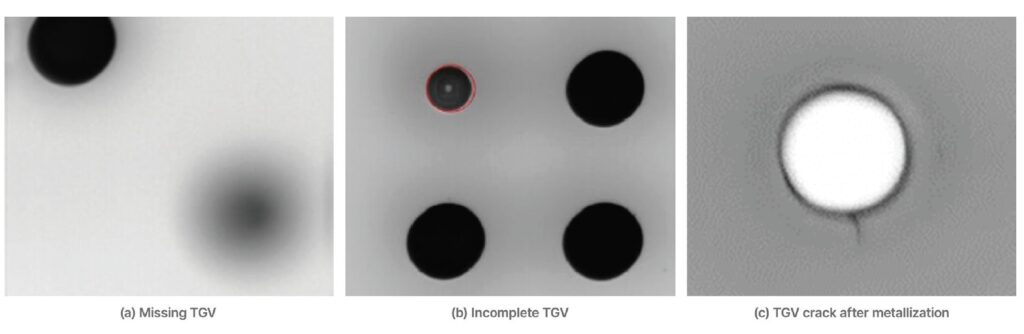
Figure 2. TGV Defect Examples (a) Missing TGV, (b) Incomplete TGV, (c) TGV crack after metallization.
These TGV process control challenges are not limited to cracks. The position accuracy of TGVs is vital for reliable electrical connections between the front and back of the glass substrate. Even slight misalignments can lead to signal integrity issues or device failure. In addition, the shape and size of the vias is another area of concern; as a result, the critical dimensions (CD) of these vias must be tightly controlled. The relationship between the top, bottom, and waist diameters of a TGV determines the profile of the via. Moreover, if the sidewall is too steep or reentrant (narrower at the bottom), it can affect the plating process, leading to incomplete metal-filled vias or voids, impacting the electrical signal performance and reliability of the final device.
Today, manufacturers are adopting a number of best practices to optimize the TGV process. On the incoming quality control front, proper process control includes identifying any defects on the surface or in the bulk of the incoming glass substrate and determining the thickness uniformity of the glass. Following each step in the TGV fabrication process, measuring critical dimensions after each process step is of imminent concern. Controlling for each of these is critical to maintaining the integrity of the final product and optimizing yields.

Figure 3: The TGV development process
In this article we will detail the entire TGV manufacturing process, starting from a bare glass panel and moving on to the fabrication of the via, TGV Cu plating, and TGV chemical mechanical planarization (Figure 3). As we discuss the process, we also will address the challenges manufacturers face at each step and expand on a unique ultra-fast laser drilling technique called laser-induced deep etching (LIDE®) that is used in the creation of vias. Afterward, we will move onto the process control solutions that enable manufacturers to reach and maintain high volume production.
TGV Manufacturing: Every Step Counts
The manufacturing of TGVs begins with a defect-free glass panel. Defects in an incoming glass panel will only compound as the TGV process moves forward. Even microscopic defects such as cracks, inclusions, scratches or surface particles can develop during manufacturing, leading to catastrophic failures. In addition, photoresist coating defects, monolayer organic residues, and variations in coating thickness can also lead to serious process control complications. Each of these issues are especially problematic in TGV manufacturing where precision and structural integrity are paramount.
Furthermore, thickness uniformity across the glass panel is key. Non-uniform thickness in a glass core substrate can significantly impact the fabrication and reliability of TGVs. As the thickness of the glass varies, the depth control during the via formation can become inconsistent, leading to incomplete or over-etched vias, increasing, for example, the variation of the waist diameter and affecting the performance of the final device. Another major issue: non-uniform substrates affect surface planarity, which is crucial for subsequent fabrication steps such as photolithography, solder bumping, and die bonding.
Following these steps, the panels undergo thorough cleaning using wet chemical and plasma-based methods to remove surface contaminants. However, this step presents several challenges. Particulate contamination, if not fully eliminated, can affect laser modification or interfere with the adhesion of subsequent layers. Additionally, any residual surface roughness can negatively impact downstream processes such as lithography and metallization, potentially compromising the fidelity of fine features.
The next step is the via formation stage. Various glass processing techniques have been used in the industry, including mechanical drilling, direct laser ablation, and lithography-based techniques with photosensitive glass followed by isotropic wet etching or deep reactive-ion etching (DRIE). A novel hybrid process utilizing laser exposure and selective wet chemical etching has been developed by LPKF Laser and Electronics SE: laser induced deep etching (LIDE).
Understanding the LIDE Technique for Via Formation
The LIDE technique is a two-step fabrication method designed to enable the high volume manufacturing of glass substrates for advanced semiconductor packaging through a combination of laser modification and selective wet chemical etching.
First, an ultrashort-pulsed laser is focused into the bulk of the glass, inducing a non-ablative modification of the material’s chemical and physical properties along a defined path. This highly localized modification, typically less than 3µm wide, spans the full thickness of the glass without removing material or introducing microcracks, thermal stress, or debris. Next, the glass panel is immersed in a chemical etchant, such as hydrofluoric acid or a hot alkaline solution. The laser-modified regions etch up to 100 times faster than the unmodified glass, enabling the formation of deep, narrow vias with smooth sidewalls and minimal tapering.
This approach allows for precise TGV formation with minimal particulate generation, no heat-affected zones, and highly uniform diameters (Figure 4). By avoiding melt ejection and suppressing microcracks, the technique helps to ensure mechanical integrity and cleanliness.
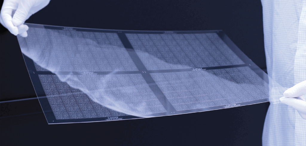
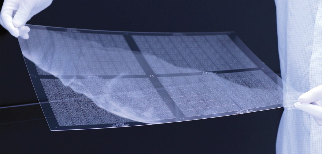
Figure 4. Glass panel with TGV. (Source: LPKF)
Post-via Processing: The Next Critical Steps
Following via formation, the substrate undergoes cleaning and surface conditioning. This includes wet chemical etching and plasma treatments to remove debris and prepare the surface for metallization. This step must be finely tuned to avoid thermal damage. Common challenges include managing heat input and debris ejection. Potential defects include microcracks from thermal stress and irregular via profiles complicating downstream metal deposition. Furthermore, the incomplete removal of debris can result in voids during the plating process, compromising the integrity of the via fill, while over-etching can damage the via walls or reduce the adhesion of subsequent layers, both of which can lead to reliability issues in the final device.
The seed layer deposition step follows. In this step a thin conductive layer, commonly Ti/Cu or Cr/Cu, is applied using sputtering or electroless plating. This layer serves as the foundation for electroplating. Challenges at this stage include achieving uniform coverage inside the high-aspect-ratio vias, which is critical for ensuring complete and reliable Cu fill. Poor surface preparation or contamination can also lead to adhesion failures, which may manifest as delamination or electrical discontinuities during device operation.
Via filling is then performed using electroplating to deposit Cu into the vias. This step must be carefully controlled to avoid common defects such as voids or seams within the Cu fill, which can compromise electrical conductivity and mechanical strength. Overplating is another concern, as it can create surface topography issues that complicate subsequent planarization and patterning steps.
Once the vias are filled, surface planarization is carried out using chemical mechanical polishing (CMP). This step removes excess Cu and the seed layer to create a flat surface. However, CMP can introduce its own set of challenges. Excessive dishing or erosion of Cu features may occur, especially if the process is not uniform across the panel. Non-uniform planarization can lead to variations in layer thickness, which may affect the performance and reliability of the final device.
Redistribution layer (RDL) formation follows. This involves photolithography, metal deposition, and etching to create the necessary interconnect patterns on the sides of the glass core. This step is highly sensitive to alignment and patterning accuracy. Misalignment with the underlying vias can result in open circuits or shorts, while defects in the patterning process can lead to electrical failures or reduced yield.
The process nears conclusion with the final singulation of the individual dies. Residual contamination, such as ionic residues, can affect long-term reliability, especially in high-performance applications. Additionally, the brittle nature of glass makes it prone to cracking during singulation, which can result in yield loss or latent reliability issues in the field.
Process Control Solutions From Start to Finish
Before the TGV manufacturing process begins, it is important to make sure the glass panel is free of inclusion defects or cracks. A laser-based scanning and optics system designed for transparent, semi-transparent, and opaque substrates, offering sub-nanometer sensitivity and the capability of all-surface inspection, can be employed to detect surface and edge defects, including particles, scratches, pits, stains, and chips, as well as monolayer organic residues. By using multiple channel inspection modes—including polarization, slope, bright field, and dark field—manufacturers can achieve sub-nanometer inspection sensitivity. In addition to inspecting the bare glass panel, it is also important to measure the thickness of the glass before starting the TGV process. Thickness uniformity across the glass panel is key.
While inspecting the glass and measuring glass thickness before manufacturing begins is of considerable importance, there are a number of specific process steps throughout the TGV fabrication and metallization process where CD metrology and defect inspection are vital. After the TGV formation step, post-process cleaning is often required to remove debris. At this step, sub-micron automatic optical inspection is used to inspect for residual particles, microcracks, or surface anomalies that can compromise subsequent metal deposition.
Besides defect detection, manufacturers need to measure CD at the top of the via, the waist of the via, and bottom of the via, along with the via’s positional accuracy relative to the design. A high-resolution, high-throughput optical panel inspection and metrology system can be used to measure these parameters for every single TGV on the panel, enabling precise monitoring of the laser and etching process. In addition, the ability to detect alternation in laser modification, incomplete etching, microcracks along individual TGVs, larger cracks between multiple TGVs, and dimples and dents on the glass surface are crucial for process optimization.
In the metallization and planarization step, inspection systems can continue to monitor for defects such as glass cracks and residues. However, there is also an additional need for 3D metrology measurements to monitor over/under plating, excess/insufficient polishing, and surface roughness, as each of these could affect overall electrical performance. An automated inspection system with integrated 3D metrology capabilities can be the preferred all-in-one solution addressing these process control requirements.
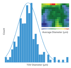
Figure 5. TGV CD distribution and analysis heat map generated by Onto Innovation’s
Discover® software.
Finally, in the inspection and yield analysis stage, the integrated use of sub-micron inspection tools and yield management software is ideally suited to support high-throughput inspection and advanced data analytics. With millions of TGVs on a panel, the ability to analyze a large quantity of inspection and metrology data within a short time period is crucial. The use of yield management software can shorten the time for analysis, identify systematic defects, and correlate process parameters with yield outcomes (Figure 5). Furthermore, manufacturers can overcome key challenges and achieve higher efficiency and yield in advanced packaging applications by automating defect classification, integrating data across systems, and enabling real-time feedback. By eliminating the need for manual review and providing consensus-based decisions, automated defect classification software can be used to enable engineers to quickly identify root causes and assess die-level quality. In addition, a robust feedback loop in which defect data is fed into analytics software allows manufacturers to make real-time process adjustments across the entire process, from the start of the process to the end.
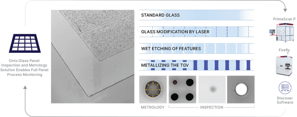
Figure 6: Full panel process monitoring includes all-surface contamination and defectivity inspection for incoming glass panel (PrimaScan™ P system) and metrology and inspection of TGVs and other defects (Firefly® system). Yield management software accelerates analysis.
Together, these solutions form a comprehensive ecosystem that supports the total TGV development process (Figure 6), enabling manufacturers to overcome key challenges and achieve higher efficiency and yield in advanced packaging applications.
Conclusion
The adoption of glass core for IC substrate is currently at the starting point of what could be considerable market growth. By 2030, glass core substrate revenue is projected to grow to $275 million, according to best case scenario results from the Yole Group. With the right tools on hand, manufacturers will be equipped to meet the rising demand for glass core substrates.
However, unlocking the full potential of glass core substrates and TGVs are not just about having tools; it is about using them in concert to build a process that is robust, repeatable, and yield optimized. As the adoption of glass as a substrate accelerates, manufacturers that invest in comprehensive process insight will be the ones that lead.
Monita Pau is Strategic and Product Marketing Director, Advanced Packaging, at Onto Innovation.

You Have a Challenge? Let’s talk.
We’d love to connect with you.
Looking to learn more about our innovative solutions and capabilities? Our team of experts is ready to assist you. Reach out today and let’s starts a conversation about how we can help you achieve your goals.
Let’s Talk
"*" indicates required fields