

Smaller Geometries, Bigger Demands: The Role of OCD in GAA Logic and Vertical Gate DRAM Process Control
AI workloads are pushing the boundaries of compute, memory, and interconnect architectures, and to meet these goals, manufacturers are rapidly accelerating advanced logic and DRAM development. Chief among these innovations: gate-all-around (GAA) logic transistor and vertical gate (VG) DRAM, two device architectures that promise higher performance, improved power efficiency, and greater scalability.
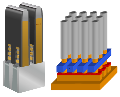
However, the arrival of these device architectures introduces new levels of manufacturing complexity brought on by increasing high aspect ratios (HAR) and the continued shrinking of device dimensions by roughly 20–30% per generation. Fortunately, new capabilities in optical critical dimension (OCD) metrology are up to the challenge of measuring and monitoring features, such as gate profiles, film thickness, and structural uniformity, at the nanometer scale. With the right tools on hand, manufacturers can maintain high volume process control for GAA logic and VG DRAM in the AI era (Figure 1).
Figure 1: GAA (left) and vertical gate DRAM (right) present new challenges for process control (pictured above)
These new capabilities are enabling the delivery of accurate, high throughput measurements across complex 3D geometries like GAA and VG DRAM by offering smaller spot size, higher signal sensitivity, and enhanced precision.
But before we discuss these new capabilities, let’s dive deeper into the challenges of both device architectures. We’ll start with GAA.
Challenges and Solutions
GAA transistors feature HAR channels and stacks of multi-layered nanosheets, in some cases as thin as 10nm. The manufacturing complexity lies in controlling individual nanowires and accurately characterizing buried nanowires within three-dimensional architectures. Precise control over nanowire dimensions is critical for achieving the desired electrical performance, including higher transistor speeds and lower power consumption. As such, GAA manufacturers need metrology solutions capable of extracting unique signals with high sensitivity and precision from each layer, even those deeply buried under semi-opaque stacks.
While GAA logic presents unique challenges in transistor scaling, VG DRAM introduces equally complex demands in memory architecture. VG DRAM involves vertical nanowire etch, multi-layer ultra-thin film deposition, sidewall trim, and buried bitlines, electrical connections that are embedded deep within the silicon substrate rather than being placed on the surface, helping reduce the footprint of each memory cell. Additionally, VG DRAM for HBM4 features smaller cell blocks. Addressing these challenges requires an OCD system with a significantly smaller spot size in order to conduct direct on-device measurements. This, unfortunately, reduces the signal strength of optical systems.
For both GAA logic and VG DRAM devices, incorporating real-time stabilization technologies and advanced optical modeling can improve measurement precision and enable tighter process windows. In addition, AI-guided analysis allows fabs to create robust measurement recipes faster and with greater accuracy for highly complex device structures like nanosheets and VG DRAM cells. Analysis software also enables more accurate measurements that are scalable across multiple tools, while supporting smart manufacturing and predictive analytics for advanced AI applications.
Many of today’s OCD metrology tools, however, have limited SNR to measure these increasingly smaller changes in the complex device structure, while other systems do not have sufficient information to separate signals from multiple parameters (e.g., dimensions from individual nanowires) in complex device structures. Furthermore, most OCD metrology systems feature large spot sizes that do not fit into the reduced DRAM cell block area for HBM4.
Without the proper advanced metrology solutions addressing these challenges, manufacturers risk variability in critical dimensions and compromising device performance and yield. As such, more data channels and enhanced SNR at higher speed are needed to overcome the reduced signal strength due to smaller geometries and increased signal complexity from higher nanowire stacks.
Onto Innovation has recently added a number of optical and algorithm innovations to its OCD arsenal, such as new multi-polarization angle data channels with real-time stabilization technologies to enhance information content and SNR. These new capabilities offer advanced optical modeling, improving measurement precision, and robustness. Furthermore, the addition of AI-guided analysis software allows fabs to create robust measurement recipes faster and with greater accuracy for highly complex device structures. This includes nanosheets and VG DRAM cells. The use of analytical software also enables more accurate measurements and is scalable across multiple tools, all in support of smart manufacturing and predictive analytics for advanced AI applications.
Conclusion
As the semiconductor industry advances toward AI-optimized architectures, the need for more precise and adaptive process control has become critical. The new OCD capabilities discussed in this blog enable tighter control over individual nanowires in GAA logic and allow for more accurate measurements within increasingly compact VG DRAM cell blocks. Combined, these innovations represent a foundational shift in how the industry measures, monitors, and optimizes the most advanced semiconductor technologies.
Jiangtao Hu is a product marketing senior director at Onto Innovation.

You Have a Challenge? Let’s talk.
We’d love to connect with you.
Looking to learn more about our innovative solutions and capabilities? Our team of experts is ready to assist you. Reach out today and let’s starts a conversation about how we can help you achieve your goals.
Let’s Talk
"*" indicates required fields