

Overlay Optimization In Advanced IC Substrates
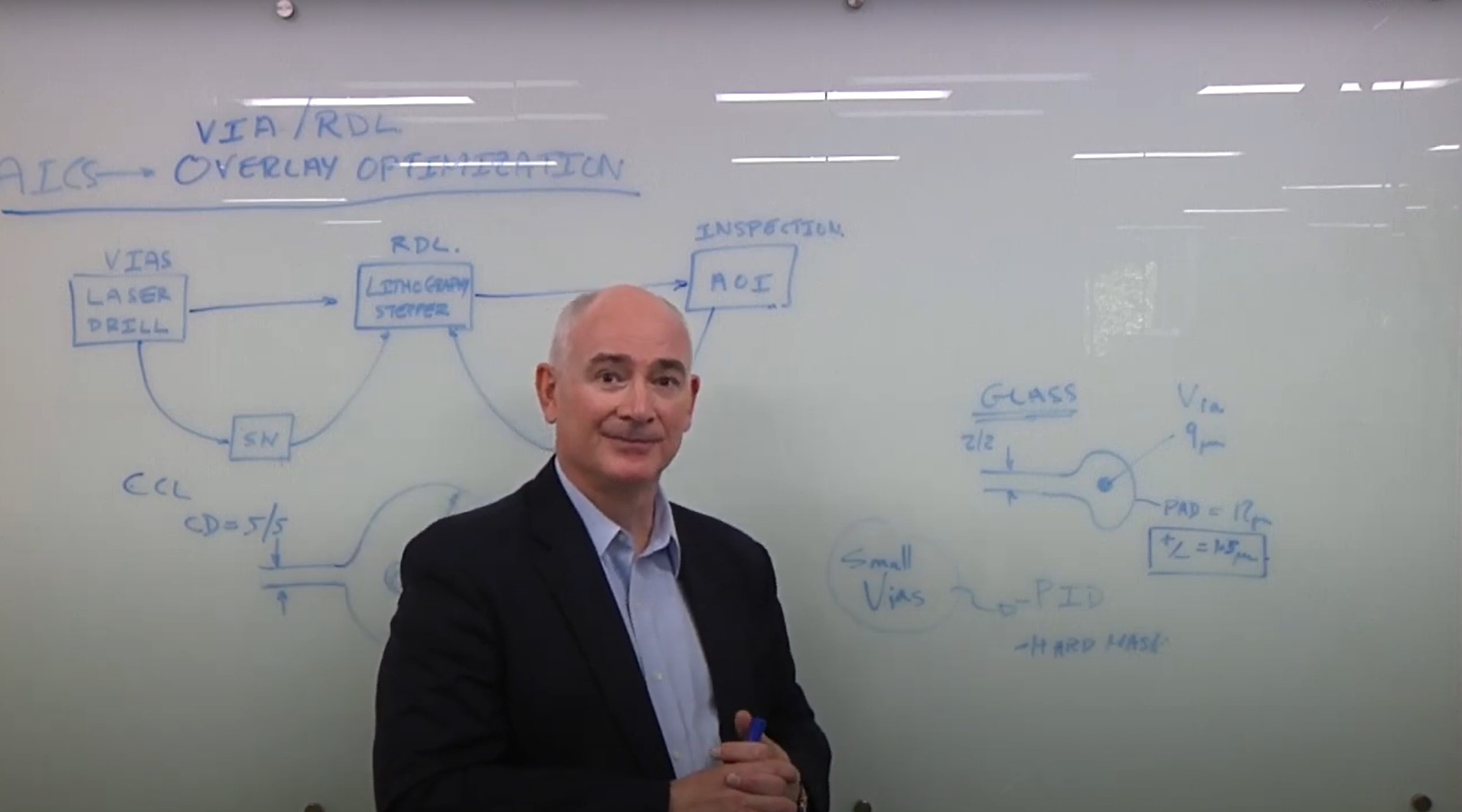
Overlay is becoming a significant problem in the manufacturing of semiconductors, especially in the world of advanced packaging substrates — think panels — the larger the area, the greater the potential for distortion due to warpage. Solving this issue requires more accurate models, better communication through feed forward/feed back throughout the flow, and real-time analytics that are baked into the process. Keith Best, director of product marketing for lithography at Onto Innovation, talks with Semiconductor Engineering about the intricacies of overlay, the pros and cons of glass substrates, and what’s needed for high-volume manufacturing.


You Have a Challenge? Let’s talk.
We’d love to connect with you.
Looking to learn more about our innovative solutions and capabilities? Our team of experts is ready to assist you. Reach out today and let’s starts a conversation about how we can help you achieve your goals.
Let’s Talk
"*" indicates required fields