

Comprehensive Process Control Solutions for Through Glass Vias
At some point in our lives, we have dropped a drinking glass or knocked over a glass-blown knickknack, only to watch it hit the floor and shatter into pieces. We learn from any early age that glass is fragile. But if glass is so fragile, why are manufacturers adopting glass core substrates?
Good question. And one that comes with a ready answer.
Glass is able to meet the new, denser line-space specifications—1.5µm and below—for interconnects that advanced logic nodes and advanced packages require. Two, glass core is better suited for large package sizes than organic substrates (Figure 1). And contrary to what those outside the semiconductor industry may think, glass substrate offers superior mechanical strength compared to its organic counterpart.
As it stands today, organic substrates will remain viable for advanced packages, but in the near future glass substrates might emerge as the preferred substrate for high-performance applications (Figure 1).
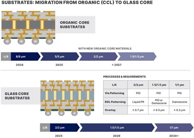
Figure 1: Roadmap for organic and glass core substrates
Through glass vias (TGVs) are the critical vertical electrical connections that pass through a glass substrate, and they require ultra-precise processing. Unfortunately, each step opens the process to a host of potential defects. Cracks, in particular, are problematic. A small crack early in the process has the potential to grow into a much larger, “killer” defect later in the manufacturing process that affects the performance and reliability of the end product.
These challenges are not limited to cracks, however. The position accuracy of TGVs is vital to ensure reliable electrical connections between the front and back of the glass substrate. Even slight misalignments can lead to signal integrity issues or device failure. In addition, the shape and size of the vias are another area of concern; as a result, the critical dimensions (CD) of these vias must be tightly controlled. The relationship between the top, bottom, and waist diameters of a TGV determines the taper angle and profile of the via. If the sidewall is too steep or reentrant (narrower at the bottom), it can affect the plating process, leading to incomplete metal-filled vias or voids, impacting the electrical signal performance and reliability of the final device.
As glass core substrates are growing in adoption, the TGV process is being rapidly developed, with process control challenges spanning the entire process. Proper process control includes ensuring the cleanliness of the incoming bare glass, determining the thickness uniformity of the glass, and measuring critical dimensions after each process step, from laser modification and chemical etching to metal filling. Control for each of these is critical to maintaining the integrity of the final product and optimizing yields.
In this blog we will explore how a combination of metrology and inspection tools, along with software analytics, can be used to help develop TGVs, beginning with the inspection of the bare glass, continuing with measuring the thickness of the glass, and following with measuring the CD of the vias themselves.
Bare Glass, Glass Thickness, and Critical Dimensions
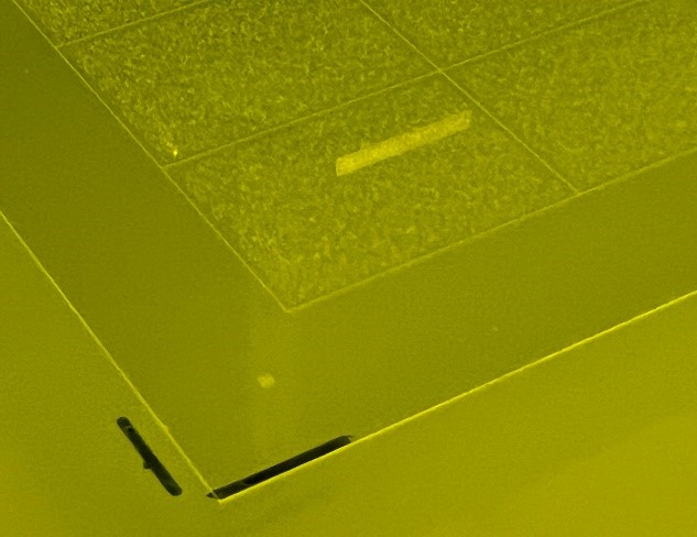
Before the TGV fabrication process even starts, it is important make sure the glass panel is free of defects (Figure 2). After all, you do not want to start off with a panel that already has an inclusion defect or crack. By using laser-based scanning and imaging optics and sensing technologies, manufacturers can reliably inspect bare glass for nanometer-sized defects, like particles, scratches, pits, and stains.
Figure 2: Glass panel with TGV.
It is also necessary to measure the thickness of the glass before starting the TGV process. Thickness uniformity across the glass panel is key. Consider this example: let us say that the thickness of a glass panel is 400µm at one end of the panel and 300µm at the other end. While this is an extreme example, you can imagine the effect that this might have on TGV height across the panel and the disastrous effect it would have on the performance of any device made from this glass substrate.
While inspecting the glass and measuring glass thickness before manufacturing begins is of considerable importance, there are a number of specific process steps throughout the TGV fabrication and metallization process where CD metrology and defect inspection are vital.
After the laser modification and etching process, manufacturers need to measure CD at the top of the via, the waist of the via, and bottom of the via;. A high-resolution, high-throughput optical panel inspection and metrology system can be used to measure these parameters for every single TGV on the panel, enabling precise monitoring of the etching process. In addition, the ability to detect defects such as incomplete etching, microcracks along individual TGV, larger cracks between multiple TGVs, and dimples and dents on the glass surface are crucial for process optimization.
In the metallization and planarization step, inspection systems can continue to monitor for defects such as residues, over/under plating, excess/insufficient polishing, and surface roughness, each of which could affect the overall electrical performance.
With millions of TGV on a panel, the ability to analyze a large quantity of inspection and metrology data within a short time period is a significant capability. The use of yield management software can shorten the time for analysis, identify systematic defects, and correlate process parameters with yield outcomes.
Conclusion
The adoption of glass core for IC substrate is currently at the starting point of what could be considerable market growth. By 2030 glass core substrate revenue is projected to grow to $275 million, according to best case scenario results from the . With the right tools on hand, manufacturers will be equipped to meet the rising demand for glass core substrates.
However, unlocking the full potential of glass core substrates and TGVs are not just about having tools; it is about using them in concert to build a process that is robust, repeatable, and yield optimized. As the adoption of glass as a substrate accelerates, manufacturers that invest in comprehensive process insight will be the ones that lead.
Monita Pau is Strategic and Product Marketing Director, Advanced Packaging, at Onto Innovation.

You Have a Challenge? Let’s talk.
We’d love to connect with you.
Looking to learn more about our innovative solutions and capabilities? Our team of experts is ready to assist you. Reach out today and let’s starts a conversation about how we can help you achieve your goals.
Let’s Talk
"*" indicates required fields