

Applications of Picosecond Laser Acoustics for Advanced Packaging
Abstract
Picosecond laser acoustic (PULSE™) Technology is an industry benchmark for metal film metrology[1]. The non-contact, non-destructive technique is well-suited for providing simultaneous multi-layer measurements in-line on product wafers. The technology has found widespread adoption across multiple device segments supporting both leading edge and specialty process monitoring and control. Thin film thickness control in advanced packaging is vital for ensuring the electrical, thermal, mechanical, and process-related performance of semiconductor devices. Inaccurate film thickness can lead to performance degradation, higher defect rates, and increased production costs, which makes precision metrology essential in the modern semiconductor manufacturing process. This paper highlights the advantages of the application of PULSE Technology in advanced packaging process monitoring.
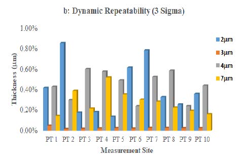
By presenting specific examples, we showcase PULSE Technology’s capability to measure multiple-layer stacks, with excellent repeatability, easy to match between tools, and long-term stability. The small spot size makes it possible for direct measurement on BUMPs for advanced packing. Recent upgrades to the system include extending the measurement range to cover very thick, rough films and improvements to signal to noise ratios making it more suitable for advanced packaging to use a single metrology tool to cover a wide range of applications. Additionally, we present examples of the non-destructive Young’s modulus measurement capability that provides critical information about the mechanical strength of the packaging material and residue detection.

You Have a Challenge? Let’s talk.
We’d love to connect with you.
Looking to learn more about our innovative solutions and capabilities? Our team of experts is ready to assist you. Reach out today and let’s starts a conversation about how we can help you achieve your goals.
Let’s Talk
"*" indicates required fields