

Achieving faster ramps/lower costs with yield prediction technology in FOPLP lithography
AI packages combine multiple advanced logic and high bandwidth memory (HBM) devices into a single architecture supporting higher I/O density, increased bandwidth, and improved power efficiency. But as AI packages grow in complexity and volume, manufacturers are under pressure to ramp quickly while maintaining high yield. For those looking to scale production of these complex packages, the economics favor approaches that improve substrate utilization and deliver more output per cycle. To accomplish this, manufacturers increasingly are adopting fan-out panel-level packaging (FOPLP) to maintain cost efficiency at scale.
Traditional wafer-based processing typically achieves approximately 55% substrate utilization with limited output per wafer. Panel-based approaches, however, can reach approximately 74% to 81% utilization, according to internal Onto Innovation estimates, while significantly increasing the number of packages produced per substrate, reinforcing the economic advantage of FOPLP at scale while improving material utilization across the substrate (Figure 1).

Figure 1: Substrate utilization efficiency improves from 55% for a 300mm wafer (supporting 6 units per substrate) to 81% for a 310×310mm panel (12 units per substrate), and reaches 74% for a 510×515mm panel (30 units per substrate).
However, FOPLP places new demands on lithography in the form of non-linear distortion, die shift, and overlay variation across the panel. These issues directly constrain yield and limit the ability of manufacturers to operate efficiently and at scale. Further complicating matters, traditional correction approaches offer ill-fitting lithography solutions for AI packaging, with most manufacturing strategies hampered by a fundamental tradeoff between yield and throughput. These challenges directly impact manufacturing cost, capacity utilization, and time to production.
Addressing these problems by conventional means can require extensive iteration to identify acceptable operating conditions. This is unacceptable for accelerated ramps to high-volume manufacturing (HVM). As a result, lithography itself has become a limiting factor in achieving consistent yield, controlling cost, and accelerating ramp time. These pressures are not incremental, however; they are structural consequences of the transition from wafer-based to panel-based manufacturing at larger formats and higher levels of integration. These challenges must be addressed for successful HVM.
In this article, we will examine how non-linear distortion and lithography correction tradeoffs hamper yield and throughput in FOPLP manufacturing and why conventional approaches impede ramp time to HVM. We will also explore how yield prediction technology enables earlier process visibility, reduces iteration, accelerates ramp, and lowers the cost of yield loss in advanced AI packaging.
Let’s start by taking a look at conventional correction strategies.

Figure 2: Heat maps of error distribution in regular FOPLP substrates. Blue regions indicate negative errors, while red regions represent positive errors. The heat maps reveal nonlinear pattern errors across the substrate.
Conventional Correction Strategies
As we mentioned earlier, in FOPLP lithography pattern errors and die shift contribute to yield loss. These errors originate during reconstitution and redistribution layer (RDL) processing and do not follow uniform distributions (Figure 2). Instead, they exhibit region-specific, non-linear spatial variation across the panel, often transitioning between positive and negative error regions. Because the distortion is non-linear and spatially non-uniform, traditional linear correction approaches cannot maintain overlay accuracy across the entire substrate. This results in localized misalignment, which directly reduces yield and introduces panel-level variability that is difficult for manufacturers to control in HVM. To address this challenge, multiple correction strategies are required to compensate for spatial variations at the exposure tool level. Unfortunately, each one introduces yield and throughput tradeoffs (Figure 3).

Figure 3: Lithography correction strategies to address the nonlinear errors in FOPLP substrate: a) Global correction: A single correction is applied uniformly across the entire substrate; b) Zone correction: The substrate is divided into zones, and corrections are applied to each zone individually; c) Die-by-die correction: Each die on the substrate is aligned and corrected individually; d) Site-by-site correction: Corrections are applied to multiple dies within a larger exposure field at once.
- Global correction applies a single adjustment across the panel. While this strategy maintains high throughput, it fails to compensate for localized errors, resulting in poor yield.
- Zone-based correction improves performance by applying localized corrections, but its effectiveness is limited, with observed yields typically ranging from 40% to 90%.
- Die-by-die correction provides the highest overlay accuracy by aligning each die individually, but this strategy is time-intensive and, as a result, reduces throughput.
- Site-by-site correction offers a partial compromise that improves yield while maintaining more practical processing times. This strategy, however, requires careful tuning. As a result, manufacturers must operate within a constrained optimization space.
In practice, selecting between these strategies requires manufacturers to balance yield targets against throughput requirements while maintaining production schedules and tool availability. Once a minimum yield threshold is defined by engineers, multiple operating points can emerge; the preferred solution is typically one that achieves acceptable yield while maximizing throughput. This is the sweet spot (Figure 4). Identifying the sweet spot requires extensive production constraints, repeated trials, and data re-analysis, resulting in increased engineering cost, extended development timelines, and delayed production ramp.

Figure 4: Determining the sweet spot in a regular lithography process requires significant time and effort because adjustments often necessitate repeated trials and data re-analysis.
Even when engineers are able to optimize this tradeoff, existing correction strategies remain fundamentally constrained. Because these strategies rely on predefined models and localized adjustments, they cannot completely compensate for complex, panel-scale distortion patterns. As a result, residual overlay errors persist, limiting achievable yield and forcing continued process optimization.
Determining optimal lithography conditions requires repeated experiments across multiple variables, including exposure settings, field configurations, and alignment strategies. Each iteration involves exposure, measurement, and analysis, increasing engineering workload, material usage, and development cycle time while extending development timelines.
Improving yield often requires adopting more granular correction strategies which inherently reduce throughput. This creates structural inefficiency: higher accuracy comes at the expense of productivity, limiting overall manufacturing output and reducing effective tool utilization in HVM environments.
Conventional workflows also rely heavily on post-lithography inspection to evaluate yield. Because defects are detected after processing is complete, corrective actions are inherently reactive, preventing manufacturers from addressing yield issues before additional process value has been added to the substrate. This results in avoidable rework, scrap, additional cycle time, and higher labor cost when excursions are detected late.
A New Strategy
To overcome these limitations, manufacturers need a new strategy that reduces reliance on iterative experimentation and enables earlier visibility into yield performance. This brings us to yield prediction technology (Figure 5).

Figure 5: Graphic depicting a yield prediction technology working scenario. An offline metrology tool captures data from a substrate, creating a comprehensive mapping dataset. The algorithms analyze the mapping data to predict overlay yield. The results are presented through a variety of visual formats, including detailed tables and graphical charts, enabling intuitive analysis, and facilitating root cause identification.
This technology addresses FOPLP lithography limitations by introducing a predictive approach to process control. Instead of relying solely on post-process inspection, this method enables manufacturers to forecast yield outcomes before lithography is completed, a clear time saver.
By combining offline metrology data with predictive analytics and machine learning algorithms, manufacturers can evaluate process performance in advance and select optimal process conditions prior to exposure and identify optimal operating conditions without extensive physical experimentation. This reduces iteration cycles, accelerates ramp, and enables manufacturers to converge on stable process conditions with fewer physical trials, while minimizing exposure to yield-driven cost risk.
Enabled through a combination of metrology data and advanced analytics, this yield prediction strategy not only predicts yield risk in the FOPLP lithography process, it supports earlier, more informed decisions on process tuning and rework and provides actionable guidance for optimizing production parameters.
The workflow for this strategy begins with offline metrology measurements that capture the detailed spatial mapping of pattern errors and die shifts across the panel. This mapping dataset provides a high-resolution representation of process variation. Predictive algorithms then analyze the data in conjunction with key process parameters, including exposure field configuration, die layout, panel layout, and overlay thresholds. Based on these inputs, the system predicts overlay error distributions and calculates expected yield performance. Then the results are presented through visualization tools, including yield dashboards, heat maps, vector plots, and histograms. With these tools at their disposal, engineers are enabled to identify the root cause of yield loss and evaluate alternative process strategies without executing full production trials. In addition, the analysis can be used to highlight dominant contributors to yield loss through more granular views such as residual overlay vector maps and axis-specific overlay error heat maps. This strategy supports faster root-cause isolation and targeted corrective action.
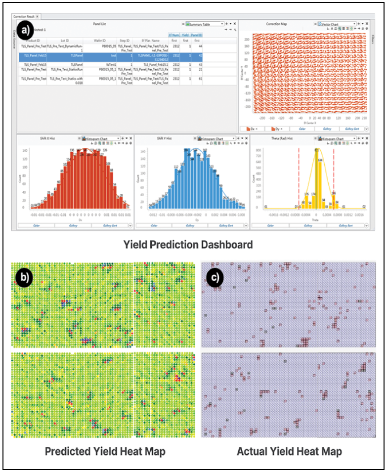
To assess the effectiveness of this predictive approach, we evaluated this strategy in HVM. Initial prediction errors ranged from 1.2% to 2.7%, demonstrating strong correlation between modeled and actual performance (Figure 6). Further analysis identified inspection variability as a key contributor to residual errors, particularly in cases involving ambiguous defect patterns requiring manual interpretation (Figure 7). Furthermore, differences in operator judgment introduced inconsistencies in measured yield results.

Figure 6: Yield prediction demonstration: a) Yield prediction dashboard: Includes predicted yield number, vector map and histogram charts for various deviations; b) Predicted yield heat map: The green dots indicate good overlay, while red and blue dots indicate overlay is out of threshold; the yield number is 97.45%; c) Actual yield heat map: The blue dots indicate good overlay, while red dots indicate the overlay is out of threshold—the actual overlay number is 98.82%. A comparison between the predicted and actual values reveals a difference of 1.37%. The results highlight opportunities for further refinement.
By standardizing inspection criteria and implementing training, this variability was reduced and prediction accuracy improved to within 0.2% to 0.8%. These results confirm predictive modeling can achieve the precision required for both development and production decision making. Beyond validation, this capability provides practical value across both development and manufacturing environments.
Accelerating Development
In development environments, yield prediction technology enables simulation-based process optimization. Engineers can evaluate multiple parameter sets, analyze overlay error behavior, and identify yield-limiting mechanisms without conducting repeated physical experiments. By reducing the number of required experiments, this approach shortens development cycles, lowers material consumption, and accelerates process qualification. It also improves the ability to understand process sensitivities and enables more targeted optimization strategies.

Figure 7: Overlay pattern variations can impact final yield due to operator errors: a) Via at pad edge; b) Via slight over pad edge; c) Good overlay. The metrology tool struggled with ambiguous patterns (e.g., see panels a and b), leading to manual judgment and variability-induced discrepancies of yield number.
Practically, this approach offers manufacturers a simulation-first workflow: teams can identify optimal parameters through simulation and then validate the predicted operating conditions using qualification substrates. This reduces both the time and cost associated with trial-and-error lithography learning (Figure 8). While these benefits are most evident during development, the impact extends further into production.
In production, yield prediction enables the earlier detection of defects within the lithography process flow, including in the coating, exposure, development, and post-treatment steps. Because early process defects can propagate through subsequent steps, the late discovery of defects can drive rework or, in some cases, permanent yield loss after additional value has already been added.

Figure 9: Visual charts and analytical tools of yield prediction technology showing: a) Various parameters for in-depth analysis; b) X-axis overlay error heat map; c) Y-axis overlay error heat map. A comparison of these maps reveals that the Y-axis exhibits the most significant overlay errors, which directly contribute to yield loss. This insight enables users to pinpoint the root cause of the issue and take corrective actions effectively, thereby improving overall process performance.

Figure 8: Vector maps of residual overlay errors are generated using yield prediction based on various process conditions. The maps are organized by shot size: a) 1×1, b) 3×3, c) 4×4, and d) 6×6. By leveraging this data-driven approach, users can accelerate process refinement, reduce trial-and-error iterations, and achieve more efficient improvements during the R&D stage, ultimately enhancing production efficiency and yield outcomes.
By enabling earlier visibility and decision-making, predictive analysis allows manufacturers to intervene before issues escalate (Figure 9). This reduces rework, limits scrap, and prevents additional value from being added to defective substrates. Equally as important, predictive analysis reduces the manpower, time, and costs associated with late-stage troubleshooting in FOPLP lithography, enabling engineering teams to respond earlier in the process and freeing them to focus on process optimization rather than reactive issue resolution.
In this way, yield prediction can be implemented as a form of preemptive quality control in mass production lines, supporting early stage screening and more reliable containment of excursions before they impact large substrate volumes (Figure 10). More importantly, yield prediction shifts defect management upstream, allowing engineers to correct for potential yield loss rather than reacting to it after completion. Taken together, these capabilities address the core constraints of FOPLP lithography.

Figure 10: The workflow of yield prediction technology for real-time, in-line process monitoring. By leveraging predictive insights, users can proactively address issues before they escalate, ensuring higher yield outcomes while minimizing rework, downtime, and associated costs.
Conclusion
FOPLP lithography is fundamentally constrained by non-linear distortion, yield–throughput tradeoffs, and the rising costs of AI packages. These challenges are compounded by conventional process control approaches that rely on iterative experimentation and post-process inspection, both of which limit ramp speed and efficiency and delay the transition to HVM.
Yield prediction technology addresses these limitations by enabling early visibility into the production process and reduces engineering reliance on trial-and-error optimization. This approach provides a practical and scalable method for improving both yield and throughput in FOPLP lithography.
By shifting process control from a reactive to predictive strategy, manufacturers can reduce yield loss, accelerate ramp to HVM, and improve overall manufacturing performance, thereby enabling more stable, cost-efficient production at scale.
Biography
John Chang is a Senior Principal Product Marketing Manager at Onto Innovation.
Jian Lu Staff is a Software Engineer at Onto Innovation.
Timothy Chang is a Senior Director of Applications Engineering at Onto Innovation.
You Have a Challenge? Let’s talk.
We’d love to connect with you.
Looking to learn more about our innovative solutions and capabilities? Our team of experts is ready to assist you. Reach out today and let’s starts a conversation about how we can help you achieve your goals.
Let’s Talk
"*" indicates required fields