

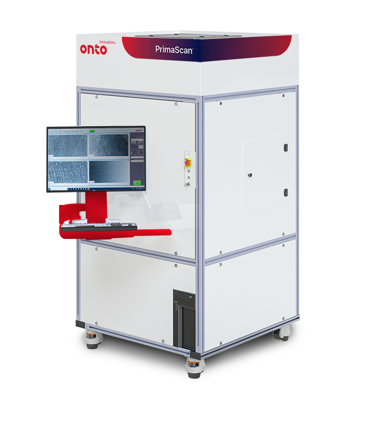
PrimaScan™ R&D System
The PrimaScan R&D System is a stand-alone, manual load version of the PrimaScan automated wafer defect and contamination inspection system that has been specifically designed with R&D and lab environments in mind.
Product Overview
The PrimaScan R&D system offers a smaller spot size and higher pixel resolution than its high volume production counterpart tools. The flexibility in sample handling options combined with the multiple sensing channels and higher resolution imaging makes this the ideal tool for R&D and lab environments. Similar to the other tools in the PrimaScan line, the PrimaScan R&D system offers reliable inspection of nanometer sized defects on a variety of opaque and transparent/semi-transparent substrates and samples suitable for either R&D or lab environments. The system can detect, measure, characterize and image surface particles, scratches, pits, bumps, surface contamination, film or bulk wafer stress, voids/inclusions, including chips and cracks at the wafer edge.
Designed with versatility in mind the PrimaScan R&D system can handle a variety of wafer sizes and substrate types including film frame, photomask and sample tray.
Applications
- Opaque or transparent wafer incoming quality (ICQ) inspection
- Process monitor wafer particle and contamination inspection
- Unpatterned blanket photoresist, dielectric or metallic coated wafer defect inspection
- Subsurface defectivity inspection for transparent and semi-transparent films and substrates
- Glass wafer defect and contamination inspection for microfluidics, microlens arrays for AR/VR/MR, flat optics, etc.
- Post-CMP or post-grind defect inspection

PrimaScan™ System
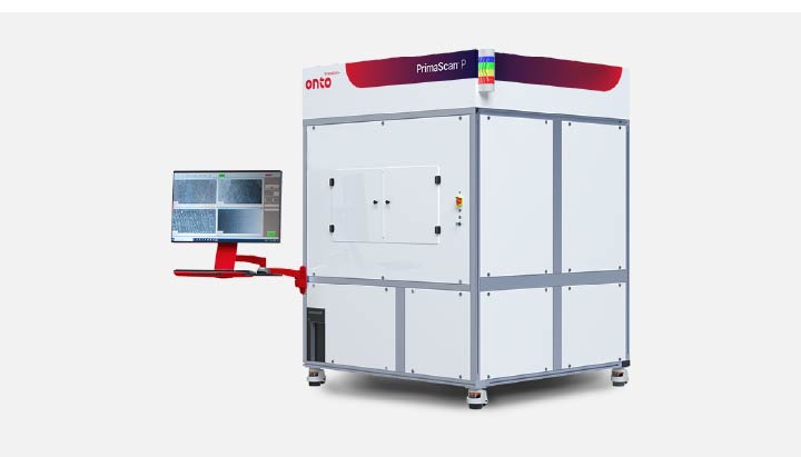
PrimaScan™ P System

Do you have a PrimaScan R&D question? Let’s talk!
As your partner for innovative solutions, we’re always here for you.
Discover how our cutting-edge semiconductor solutions are engineered to meet your most complex challenges: delivering performance, reliability and innovation where it matters most.
Let’s Talk
"*" indicates required fields