

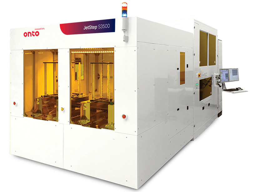
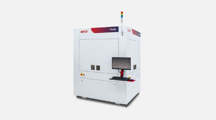
JetStep® S3500 System
The JetStep S3500 system is designed to provide OSATS with a high-volume manufacturing advanced packaging lithography solution. For substrates up to 720mm x 600mm, it supports fan-out panel level packaging.
Product Overview
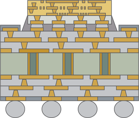
The JetStep S3500 panel lithography system is specifically designed for advanced packaging panel production. As fan-out packages increase in size and complexity, requiring panel substrates instead of wafers, the JetStep S3500 system addresses these challenges with advanced features. It handles die shift caused by placement accuracy errors, CTE mismatch and panel warpage. The system incorporates a large exposure field (59.4 x 59.4mm) with resolution capability to 2/2 L/S and options for increased resolution to 1/1. In addition, it supports multiple exposure wavelengths, ideal for process development with new photosensitive polymers. Application-specific options include warped panel handling, “on-the-fly” optical focus, and die shift correction (StepFAST™ Solution), helping to ensure precise and reliable panel-level packaging.
Applications
- Fan-out panel level packaging (FOPLP)
- Interposers
- Photo imageable Dielectric (PID) vias
- Redistribution lines (RDL) / Under bump metallization (UBM)
- Non-standard substrates
Featured Markets
Adaptive Shot Lithography Solution
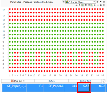
Die shift on reconstituted panels can significantly impact both productivity and yield. To address this challenge, we use a parallel die placement measurement process and advanced analytics to provide a means to balance productivity against yield. Our integrated lithography cell, featuring Firefly inspection, StepFAST software, and JetStep Lithography, delivers industry-leading throughput and yield for fan-out panel level packaging.
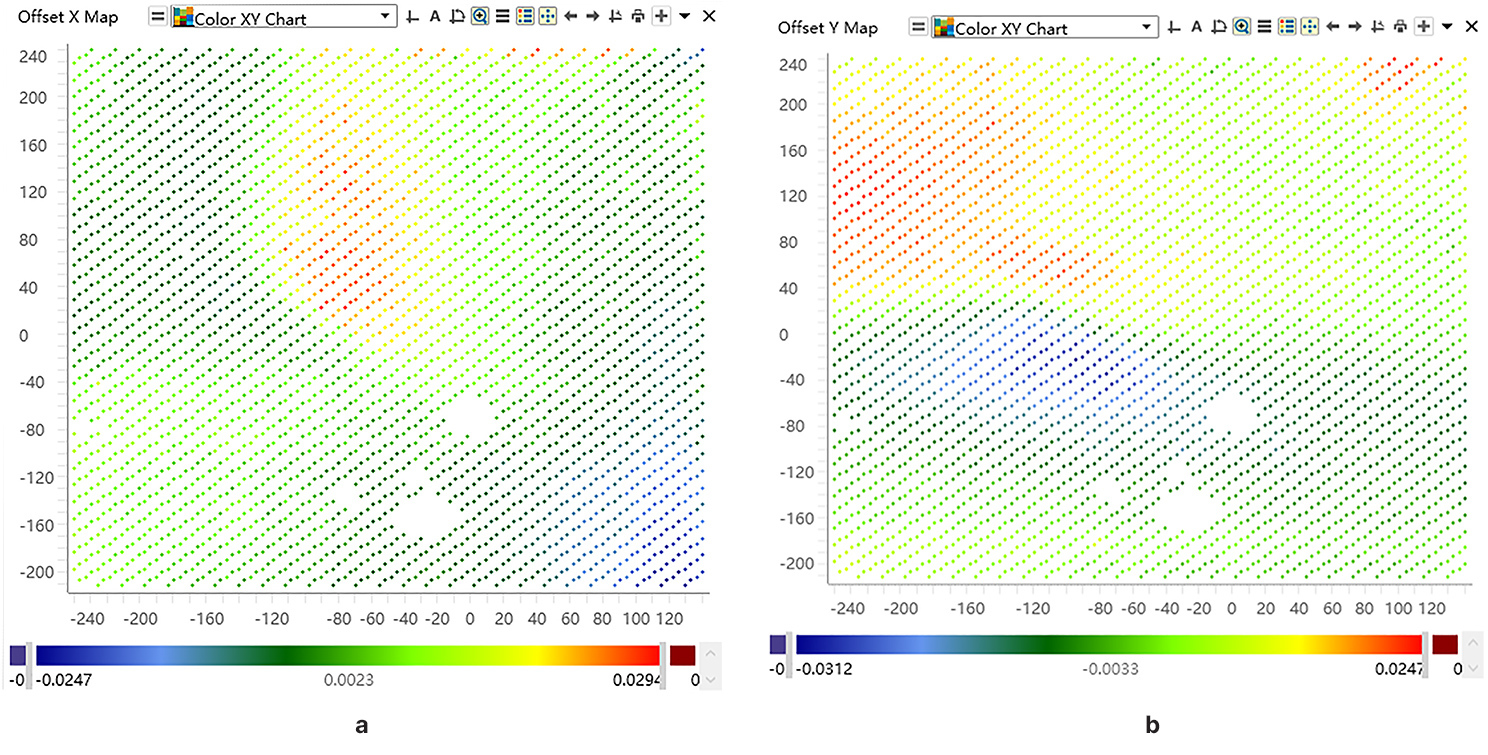
Overcoming FOPLP Die Placement Error
It is well understood that advanced packaging applications require high performance, low cost, increased functionality and improved reliability that 2.5D and 3D packaging solutions provide. Fan-out panel-level packaging (FOPLP) is one of the technologies that has the potential to meet these packaging requirements.
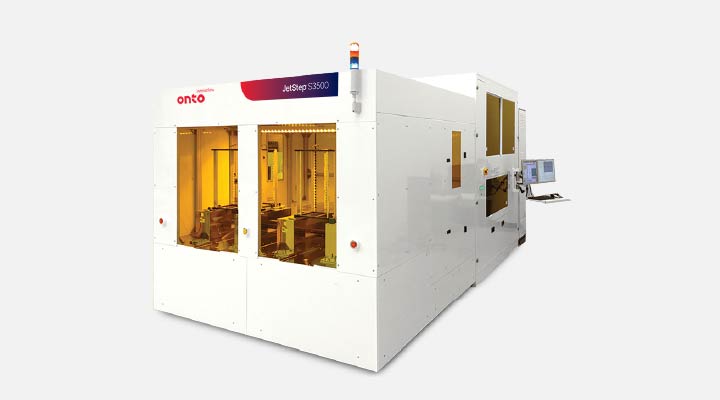
JetStep® S3500 System
The JetStep S3500 system is designed to provide OSATS with a high-volume manufacturing advanced packaging lithography solution. For substrates up to 720mm x 600mm, it supports fan-out panel level packaging.
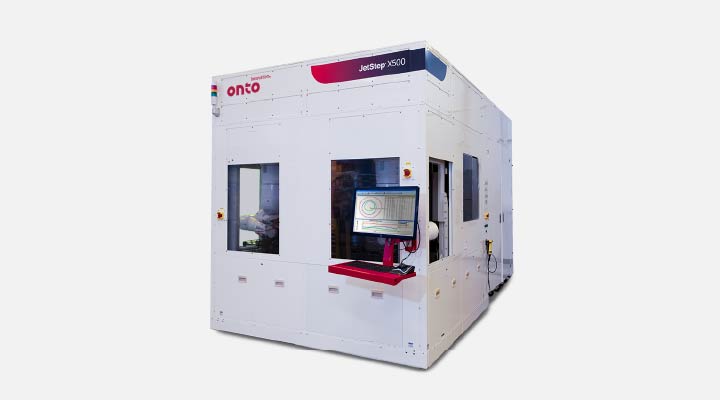
JetStep® X500 System
The JetStep X500 system is designed to provide AICS and OSAT manufacturers with a high-volume manufacturing lithography solution for heterogeneous integration. The JetStep X500 system exposes panel-type substrates made of CCL, FR4, composite, glass or other materials.
Firefly® G3 System
The Firefly G3 system provides automated inspection and 3D metrology for advanced IC substrates and panel level packaging, delivering high resolution and productivity for demanding applications like high-performance computing (HPC), artificial intelligence (AI), cloud computing and machine/deep learning.

StepFAST® Software
An advanced feed-forward lithography software solution for fan-out panel level packaging that enhances yield and throughput by correcting die placement errors through external measurements, predictive analytics and adaptive shot control.
JetStep® X500 System
StepFAST® Software
The Great Lithography Debate: Copper Clad Laminate or Glass Substrates?
Adaptive Shot Technology To Address Severe Lithography Challenges For Advanced FOPLP
Overcoming FOPLP Die Placement Error

Do you have a JetStep S3500 question? Let’s talk!
As your partner for innovative solutions, we’re always here for you.
Discover how our cutting-edge semiconductor solutions are engineered to meet your most complex challenges: delivering performance, reliability and innovation where it matters most.
Let’s Talk
"*" indicates required fields