

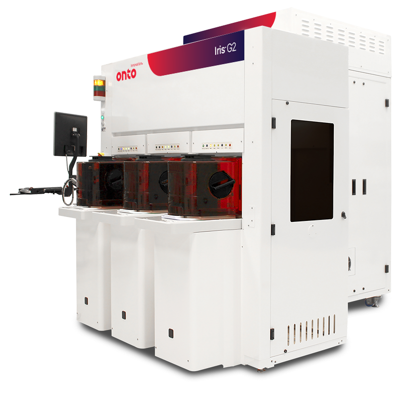
Iris™ G2 System
The Iris G2 system is an advanced optical metrology tool for both common and critical thin films for advanced node, mature and specialty devices, enabling manufacturers to increase transistor speed, reduce power consumption and improve reliability.
Product Overview
As semiconductor device technologies become increasingly complex, requiring thinner and more uniform films, the need for a stable, all-in-one thin film metrology solution becomes a necessity. By controlling the quality and effective thickness of gate films, the Iris G2 system supports critical device scaling and performance improvements.
For ultra-thin multilayer films measuring 10Å to 50Å, the Iris G2 system features deep ultraviolet (DUV) spectroscopic ellipsometry (SE) for common films and coupled proprietary laser ellipsometry technologies for critical films, providing customers with the flexibility to optimize cost of ownership, better stability, and ease of operation in a versatile tool for specialty, mature and advanced logic and memory processes.
Additionally, a single platform simplifies fleet management and fab operations while reducing overall capital investment.
Applications
- Critical film measurement
- Common film measurement
- 2D and 3D OCD measurement
- Wafer bow, warp, and film stress
Intelligent Line Monitoring & Control with Integrated Metrology
Enhance CMP process control with a connected metrology approach that feeds forward data from standalone OCD or films metrology to integrated metrology, connected through AI-driven analytical software. This approach, powered by advanced modeling and analysis tools, can deliver high-precision, high-throughput results—minimizing or eliminating the need for and cost of new TEM data and enabling accelerated time to solution, faster excursion detection, reduced cost and improved Cpk.

Enhancing CMP Process Control with Intelligent Line Monitoring & Integrated Metrology
As semiconductor manufacturers push the boundaries of performance and functionality—driven by high-performance computing and AI applications—chemical mechanical planarization (CMP) processes increase in intensity complexity. New logic transistor designs, 3D NAND stacking, and DRAM integration introduce more CMP layers and tighter process windows.

IMPULSE® V System
The IMPULSE V system helps to advance CMP processing with enhanced wavefront technology and AI-driven analytics, delivering over 2X precision improvement and faster solutions, crucial for next-gen semiconductor manufacturing demands.

IMPULSE®+ System
The IMPULSE+ system is designed to deliver film measurement, fidelity and productivity in the CMP process module. Available as an integrated or standalone platform, it offers high sensitivity and accuracy.

Atlas® V System
The Atlas V system is an OCD and thin film metrology tool for high volume manufacturing, enabling FinFET & Gate-All-Around (GAA) logic, DRAM, and 3D NAND device process control.

Atlas® III+ System
The Atlas III+ system provides dependable OCD and thin film metrology for established technologies, with flexible performance across a wide range of process layers and device types.
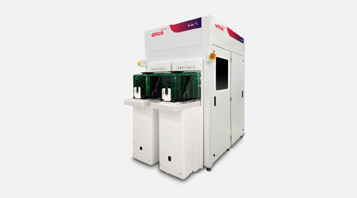
Iris™ S System
The Iris S system is a versatile platform solution for the advanced packaging and specialty market, supporting 150mm, 200mm and 300mm wafers. It provides thin and thick film, OCD and wafer bow and film stress measurements.
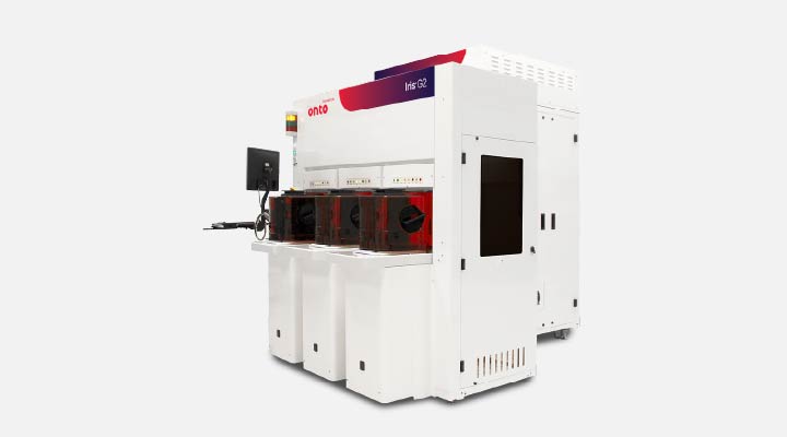
Iris™ G2 System
The Iris G2 system is an advanced optical metrology tool for both common and critical thin films for advanced node, mature and specialty devices, enabling manufacturers to increase transistor speed, reduce power consumption and improve reliability.

OCD Solutions
A suite of OCD modeling software and computing hardware that enables the full capability and connectivity across all Onto OCD and thin film metrology systems, including Atlas, Aspect, Iris and IMPULSE systems.
Iris™ S System
IMPULSE® V System
IMPULSE®+ System
Atlas® V System
Atlas® III+ System
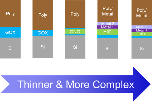
Measuring Multi-Layer Ultra-Thin Critical Films

Do you have an Iris G2 system question? Let’s talk!
As your partner for innovative solutions, we’re always here for you.
Discover how our cutting-edge semiconductor solutions are engineered to meet your most complex challenges: delivering performance, reliability and innovation where it matters most.
Let’s Talk
"*" indicates required fields