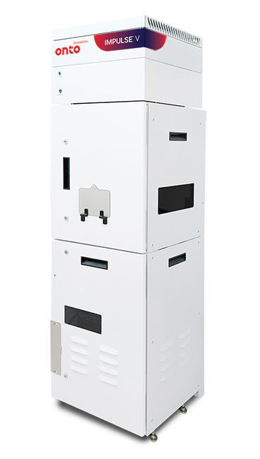
IMPULSE® V System
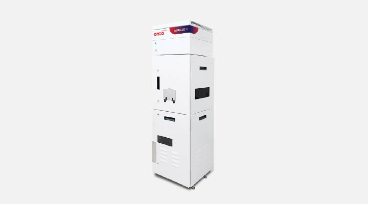
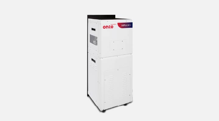
The IMPULSE V system helps to advance CMP processing with enhanced wavefront technology and AI-driven analytics, delivering over 2X precision improvement and faster solutions, crucial for next-gen semiconductor manufacturing demands.
Product Overview
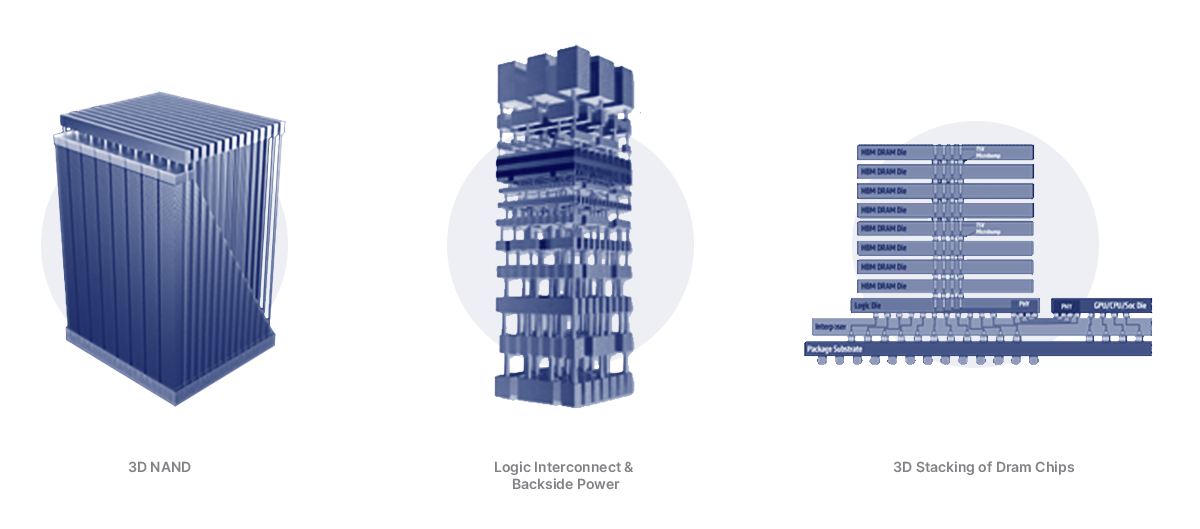
As wafer uniformity requirements tighten and vertical scaling increases, the need for CMP processing grows across market segments. Logic introduces new transistor designs and materials, DRAM incorporates new materials and process steps to planarize, and 3D NAND adds more decks, stacks and tiers.
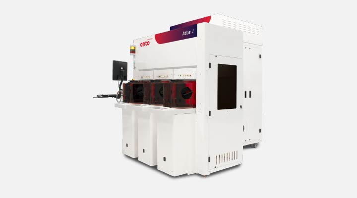
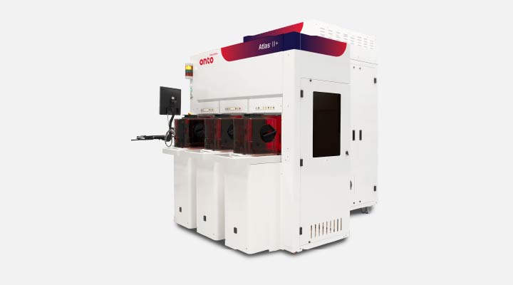
The IMPULSE V system, available as an integrated or standalone platform, enhances film measurement fidelity and productivity for the CMP process module. With deep ultraviolet (DUV) optics and AI-driven machine analytics derived from our Atlas® platform, it works in conjunction with the Atlas® platform to provide CMP process engineers the capability to manage excursions and drive process improvement (Cpk.).
Advanced wavefront technology suppresses previous layer noise in complex structures. It provides feedback to improve long term repeatability. Designed for higher sampling, in-die/on-device and wafer edge measurements, the system offers improved reliability, higher throughput and over 2X precision improvement compared to the previous generation. Onboard AI-driven machine learning uses a signal-to-noise ratio for faster time-to-solution, addressing layers that were previously challenging to measure.
Applications
- CMP
Intelligent Line Monitoring & Control with Integrated Metrology
Enhance CMP process control with a connected metrology approach that feeds forward data from standalone OCD or films metrology to integrated metrology, connected through AI-driven analytical software. This approach, powered by advanced modeling and analysis tools, can deliver high-precision, high-throughput results—minimizing or eliminating the need for and cost of new TEM data and enabling accelerated time to solution, faster excursion detection, reduced cost and improved Cpk.
Enhancing CMP Process Control with Intelligent Line Monitoring & Integrated Metrology
As semiconductor manufacturers push the boundaries of performance and functionality—driven by high-performance computing and AI applications—chemical mechanical planarization (CMP) processes increase in intensity complexity. New logic transistor designs, 3D NAND stacking, and DRAM integration introduce more CMP layers and tighter process windows.
Hybrid Bonding Process Control Solution
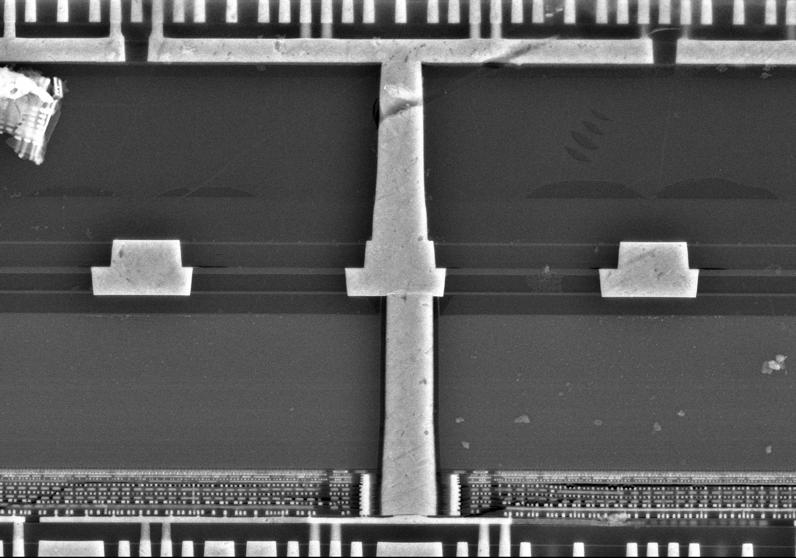
Hybrid bonding enables ultra-dense 3D memory interconnects with up to 1,000x more connections than microbumps. Achieving high yield requires stringent process control, including monitoring topography and detecting particles, cracks and voids. Measuring dishing in copper pads provides valuable insight into surface conditions. Together, these process control insights contribute to improved device reliability and performance.
Enabling In-Line Process Control for Hybrid Bonding Applications
As demand grows for high-performance computing (HPC) and AI-driven applications, manufacturers are turning to hybrid bonding to enable the ultra-dense 3D integration required for next-generation chip architectures. This advanced packaging technology presents significant process challenges. Surface preparation must be precisely controlled to eliminate particles, excess recess, and copper pad dishing, all of which can compromise bond quality. During pre-annealing, particle-induced gaps and wide bonding gaps can prevent proper wafer contact. Post-annealing, the formation of dielectric and metal voids introduces further risks to electrical performance and long-term reliability.
Do you have an IMPULSE V system question? Let’s talk!
As your partner for innovative solutions, we’re always here for you.
Discover how our cutting-edge semiconductor solutions are engineered to meet your most complex challenges: delivering performance, reliability and innovation where it matters most.
Let’s Talk
"*" indicates required fields
