

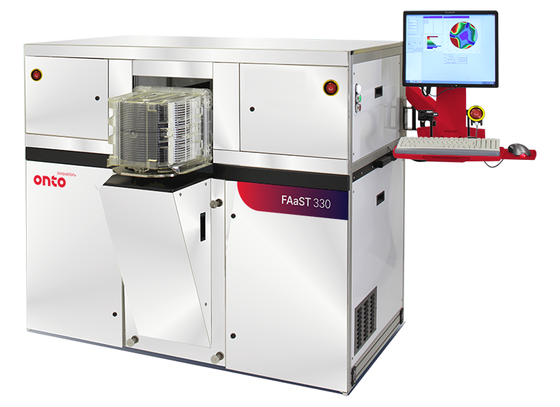
FAaST® Digital SPV System
The FAaST Digital SPV system provides a fast, non-contact, and preparation-free method for full wafer imaging of contamination in silicon. High resolution maps of diffusion length and iron (Fe) concentration are generated in minutes, setting the industry standard for precision and sensitivity in Fe contamination control, reaching the E7 cm-3 range.
Product Overview
There is no disputing the detrimental effect of metallic contamination on the integrity of the critical gate oxide used in integrated circuits. During high temperature processing, contamination in the silicon wafer often precipitates at the Si/dielectric interface or segregates into the dielectric—both scenarios can cause premature device failure and reduced yield. As device dimensions shrink, the tolerance for contamination decreases, requiring ever-lower background levels of metals like iron (Fe). Over the past 25 years, the IC industry has reduced typical Fe concentrations by more than three orders of magnitude, yet further reduction is essential, especially for applications like CMOS image sensors.
The FAaST Digital SPV system addresses this challenge with industry-leading sensitivity and speed. It provides a fast, non-contact, and preparation-free method for full-wafer imaging of contamination. High-resolution maps of minority carrier diffusion length and Fe concentration are generated in minutes, enabling fabs to detect and control contamination at levels as low as the E7 cm⁻³ range.

Figure 1. Typical background Fe concentration in new IC Fablines (blue) and the state-of-the-art SPV detection limit (red)
Applications
- Ingot qualification
- Outgoing / incoming polished wafers
- Epitaxy
- Cleaning
- Diffusion furnace monitoring
- Rapid thermal anneal
Featured Markets
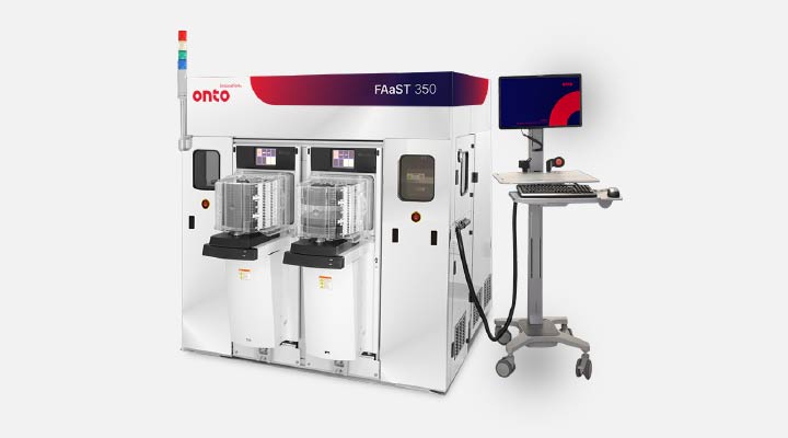
FAaST® CV/IV System
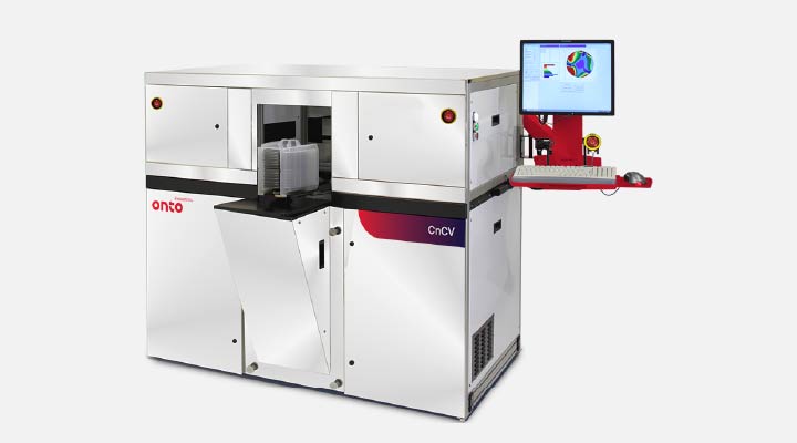
CnCV® System

Do you have a FAaST Digital SPV system question? Let’s talk!
As your partner for innovative solutions, we’re always here for you.
Discover how our cutting-edge semiconductor solutions are engineered to meet your most complex challenges: delivering performance, reliability and innovation where it matters most.
Let’s Talk
"*" indicates required fields