

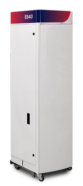
EB40™ Module
The EB40 Module combines edge and backside inspection into one tool with the option to be paired with an inspection system to provide a high throughput all surface inspection solution.
Product Overview
The Class 1 certified EB40 module offers combined edge and backside inspection and is also available as separate edge (E40) and backside (B40) modules. These modules provide brightfield and darkfield inspection to detect defects on the entire bevel and backside, covering Zone 1 to Zone 5. This enables faster root-cause analysis of defects that can migrate to the wafer interior, impacting die yield.
The EB40 module captures defect images on the fly, creates whole-wafer composite images, and integrates with SEM bevel review. All inspection and metrology results, including defect, whole wafer and SEM images can be analyzed together in a single database using Discover Defect software. Correlating EBR metrology with defectivity data, SEM data and micro-inspection results is just the beginning of what Discover software can do. In addition to advanced on-tool defect binning, real-time edge ADC classification can be assigned to defects prior to manual offline review using Discover Review software.
Applications
- EDGE INSPECTION
- Lithography process monitoring
- Cracks/Chips, Slurry, cleaning contaminants and residual films
- EBR Metrology
- Bonded wafer adhesive inspection
- BACKSIDE INSEPCTION
- Scratches
- Chuck and end effector signatures
- Backside particles and residues
- Wafer level pattern detection
Featured Markets

Dragonfly® G5 System

Dragonfly® G3 System
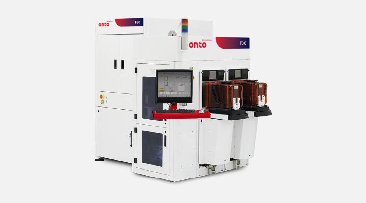
F30™ System
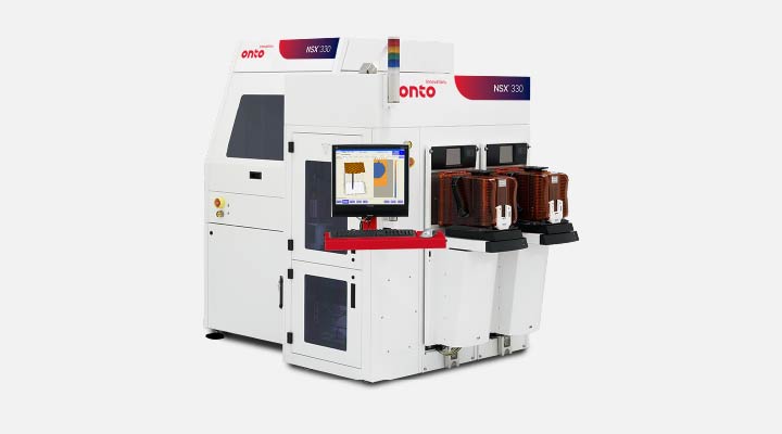
NSX® 330 System

Discover® Defect Software

Discover® Review Software

Enabling In-Line Process Control for Hybrid Bonding Applications

Do you have an EB40 module question? Let’s talk!
As your partner for innovative solutions, we’re always here for you.
Discover how our cutting-edge semiconductor solutions are engineered to meet your most complex challenges: delivering performance, reliability and innovation where it matters most.
Let’s Talk
"*" indicates required fields