
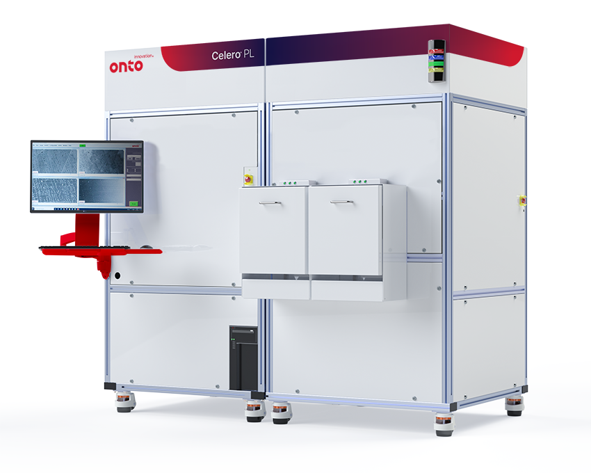
Celero™ PL System
The Celero PL system is designed for subsurface defect inspection and classification for silicon carbide (SiC) and gallium nitride (GaN) based wafers and compound semiconductor materials.
Product Overview
The Celero PL system utilizes a laser-based phase detection and imaging capability that leverages custom optics and image processing algorithms to enable best in class throughput and sensitivity for silicon carbide and gallium nitride-based materials on 100mm to 300mm wafer sizes. Leveraging multiple light sources and sensor channels, the system can detect, measure and image a broad variety of subsurface crystalline defects, associated with bulk wafers and epitaxial layers, surface particles, scratches, pits, surface contamination, stains, point or bulk wafer stress, voids/inclusions, including chips and cracks at the edge of the wafer.
Applications
- Frontside / backside / edge / subsurface defectivity and contamination
- Crystalline defectivity in III-V substrates and epitaxial layers
- Thick wafer / seed wafer surface and sub-surface defectivity
- Substrate-to-epitaxial layer defect mapping (sub-defect mapping)
- Wafer based microLED / VCSEL / EE laser materials
Featured Markets

PrimaScan™ System

PrimaScan™ R&D System

Do you have a Celero PL system question? Let’s talk!
As your partner for innovative solutions, we’re always here for you.
Discover how our cutting-edge semiconductor solutions are engineered to meet your most complex challenges: delivering performance, reliability and innovation where it matters most.
Let’s Talk
"*" indicates required fields